Array substrate, manufacturing method of the same, and fabricating method of liquid crystal display device including the array substrate

Active Publication Date: 2007-01-04
LG DISPLAY CO LTD
View PDF5 Cites 27 Cited by
  • Summary
  • Abstract
  • Description
  • Claims
  • Application Information

AI Technical Summary

Benefits of technology

[0027] An advantage of the present invention is to provide an array substrate and a manufacturing method of the same that improve a test process and reduce manufacturing costs.
[0028] Another advantage of the present invention is to provide a fabricating method of a liquid crystal display device having improved productivity.
[0029] Additional features and advantages of the invention will be set forth in the description which follows, and in part will be apparent from the description, or may be learned by practice of the invention. The advantages of the invention will be realized and attained by the structure particularly pointed out in the written description and claims hereof as well as the appended drawings.
[0030] To achieve these and other advantages and in accordance with the purpose of the present invention, as embodied and broadly described, a manufacturing method of an array substrate for a liquid crystal display device includes preparing a substrate including a display area and a non-display area, forming gate and data lines in the display area on the substrate, wherein the gate and data lines cross each other to define a pixel region, forming a thin film transistor at each crossing of the gate and data lines, forming a pixel electrode to the thin film transistor in the pixel region, forming first and second gate shorting bars in the non-display area and electrically connected to the gate lines, forming first and second data shorting bars in the non-display area and electrically connected to the data lines, forming n gate probe test lines (where n is an integer) in the non-display area, forming m data probe test lines (where m is an integer) in the non-display area, forming first connection patterns connecting the gate lines and the n gate probe test lines, and forming second connection patterns connecting the data lines and the m data probe test lines, wherein the gate lines include n gate gro

Problems solved by technology

Therefore, manufacturing costs are increased.
Thus, various needle frames are required, and needle f

Method used


Image

  • Array substrate, manufacturing method of the same, and fabricating method of liquid crystal display device including the array substrate
  • Array substrate, manufacturing method of the same, and fabricating method of liquid crystal display device including the array substrate
  • Array substrate, manufacturing method of the same, and fabricating method of liquid crystal display device including the array substrate

Examples


Embodiment Construction

[0043] Reference will now be made in detail to embodiments of the present invention, examples of which are illustrated in the accompanying drawings.

[0044]FIG. 4 is a plan view illustrating an array substrate according to the present invention.

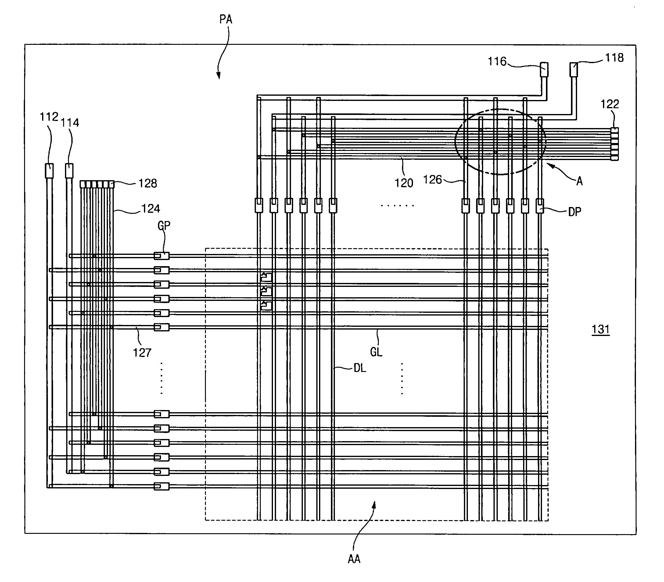
[0045] In FIG. 4, a display area AA, which may be referred to as an active area, and a non-display area PA, which may be referred to as a pad area, are defined on a substrate 131. Gate lines GL and data lines DL are formed in the display area AA and cross each other to define pixel regions. A thin film transistor and a pixel electrode connected to the thin film transistor are formed in each pixel region. Gate pads GP are formed at one ends of the gate lines GL and are disposed in the non-display area PA. Data pads DP are formed at one end of the data lines DL and are disposed in the non-display area PA.

[0046] To prevent static electricity, first and second gate shorting bars 112 and 114 and first and second data shorting bars 116 and 118 are...


PUM


Abstract

A manufacturing method of an array substrate for a liquid crystal display device includes among other features, preparing a substrate including a display area and a non-display area, forming first and second gate shorting bars in the non-display area and electrically connected to gate lines, forming first and second data shorting bars in the non-display area and electrically connected to data lines, forming n gate probe test lines in the non-display area, forming m data probe test lines in the non-display area, forming first connection patterns connecting the gate lines and the n gate probe test lines, and forming second connection patterns connecting the data lines and the m data probe test lines, wherein the gate lines include n gate groups connected to the n gate probe test lines, respectively, and wherein the data lines include m data groups connected to the m data probe test lines, respectively.

Description

[0001] The present invention claims the benefit of Korean Patent Application No. 2005-0057484 filed on Jun. 30, 2005, which is hereby incorporated by reference for all purposes as if fully set forth herein. BACKGROUND OF THE INVENTION [0002] 1. Field of the Invention [0003] The present invention relates to a liquid crystal display (LCD) device. More particularly, the present invention relates to an array substrate, a manufacturing method of the same and a fabricating method of a liquid crystal display device including the array substrate. [0004] 2. Discussion of the Related Art [0005] Liquid crystal display (LCD) devices use the optical anisotropy and polarization properties of liquid crystal molecules to produce an image. Liquid crystal molecules have a definite alignment as a result of their long, thin shapes and are arranged to have initial pretilt angles. The alignment direction can be controlled by applying an electric field. Specifically, variations in an applied electric fiel...

Claims


Application Information

Patent Timeline
IPC IPC(8): G02F1/1333
CPCG02F1/1345
Inventor KIM, JEOM-JAESONG, MOO-HYOUNGPARK, CHANG-BAELEE, JUNG-EUN
Owner LG DISPLAY CO LTD
Why Eureka
Try Eureka