Measurement of the top surface of an object with/without transparent thin films in white light interferometry
a technology top surface measurement, applied in the field of white light interferometry or vertical scanning phaseshift interferometry, can solve the problem that the known methods of wli lose the ability to profile surfaces with such superimposed interferograms
- Summary
- Abstract
- Description
- Claims
- Application Information
AI Technical Summary
Problems solved by technology
Method used
Image
Examples
Embodiment Construction
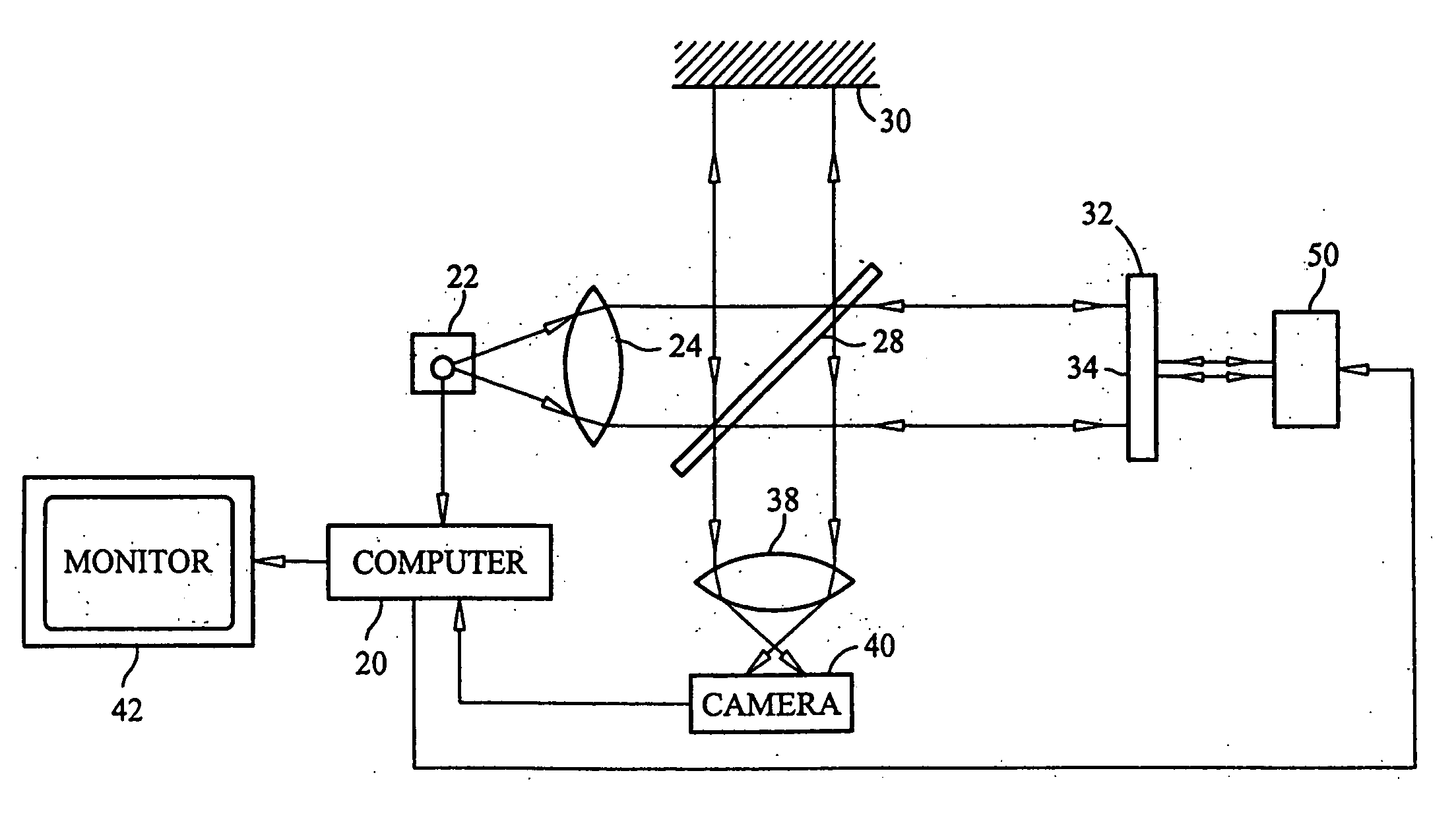
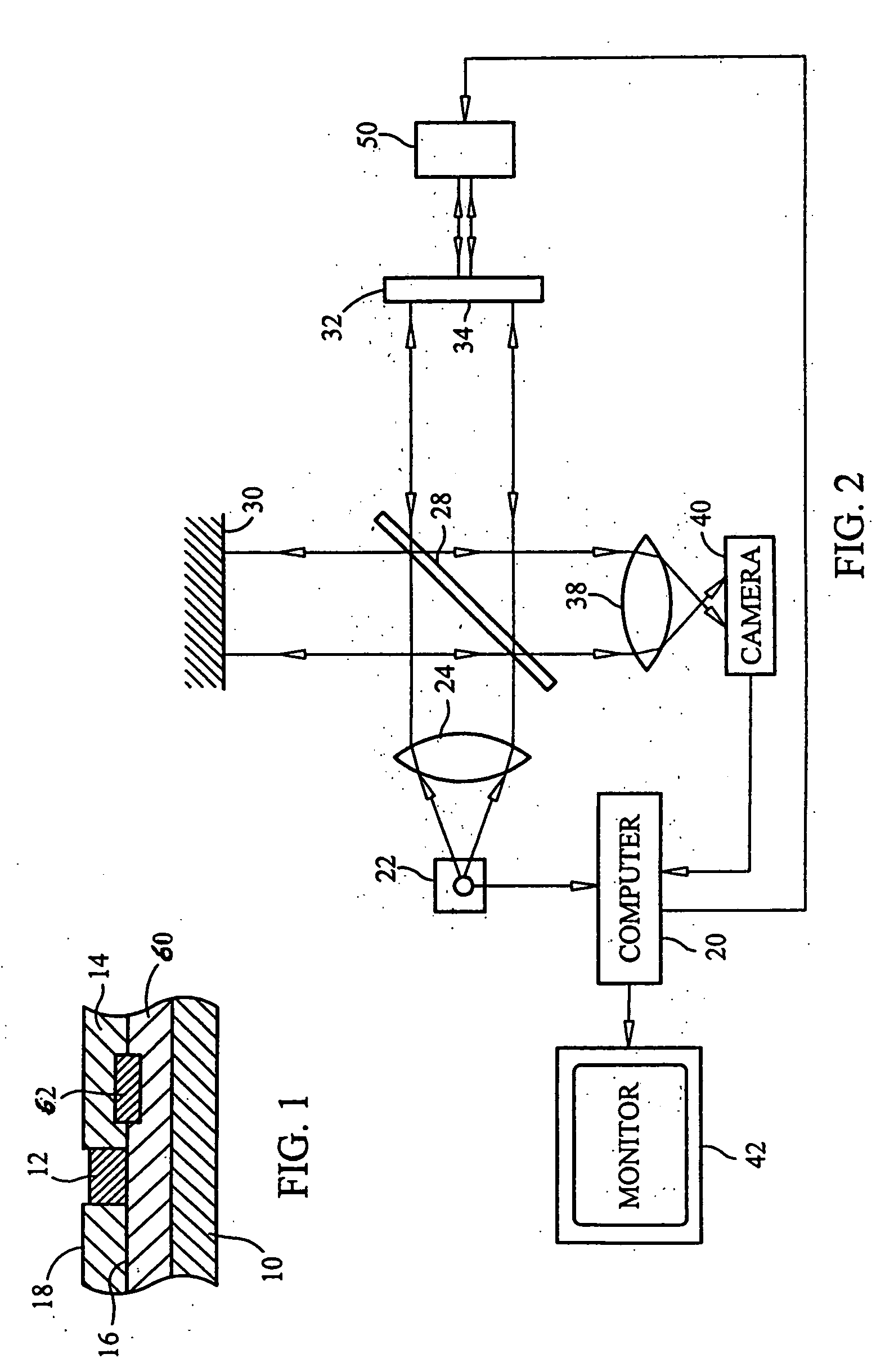
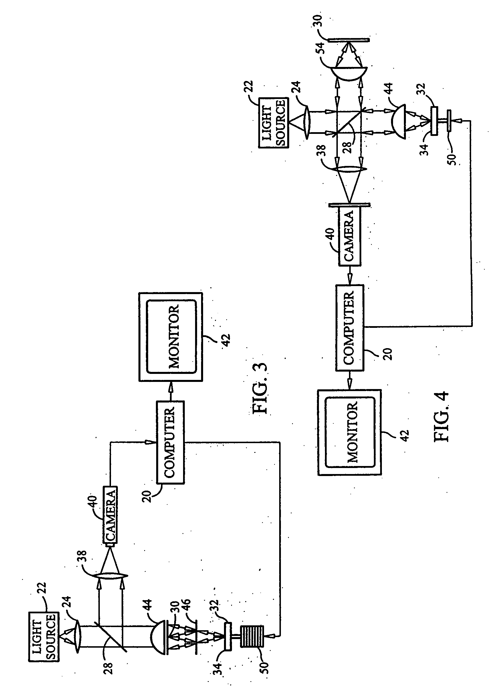
[0012] Reference now should be made to the drawings, in which the same reference numbers are used throughout the different figures to designate the same or similar components. FIG. 1 is a cross section of a portion of a test surface or objective where the measuring surface is covered with a transparent layer of a thin film. FIG. 1 is representative of an objective which may be of a variety of different types including, but not limited to, a CMP pattern wafer 70. Such a wafer includes a substrate 10 on which metallization regions, such as the patterns 12 and 62, are located. The top surface of the pattern 12 is exposed. As illustrated in FIG. 1, a thin transparent film 14 is located over much of the entire surface of the wafer 70, with the uppermost or top surface position 18 located higher than the metallization regions 12, and with a second reflective surface 16 at the boundary between the thin film 14 and the region 60. It also should be noted that for some applications, such as s...
PUM
 Abstract
Description
Claims
Application Information


