Non-contact type micro-nano 3D measuring method and device

A three-dimensional measurement, non-contact technology, applied in the direction of measuring devices, optical devices, instruments, etc., can solve the problems of inability to distinguish finer shape features, unsuitable for large-scale production environments, and inability to use industrial measurement, etc., to achieve high The effect of high-precision three-dimensional shape measurement, expanding the longitudinal measurement range, and shortening the overall measurement time

Inactive Publication Date: 2016-06-15
淮安普瑞精仪科技有限公司
View PDF5 Cites 14 Cited by
  • Summary
  • Abstract
  • Description
  • Claims
  • Application Information

AI Technical Summary

Problems solved by technology

[0008] Scanning electron microscopy is the most common tool for micro-nano three-dimensional measurement, but almost all non-conductive samples need to be coated with a thin layer of conductive material on the surface when measured by this method, which will lead to bending and deformation of the device, especially For free-standing structures, such as cantilever beams, and scanning electron microscope testing is time-consuming and not suitable for mass production environments
[0009] The three-coordinate measuring machine is an important tool for measuring the dimensional accuracy of industrial products. In recent years, with the rapid development of micro-nano processing technology, the feature size of devices and the associated tolerances have been continuously reduced, especially for the semiconductor industry, the detection accuracy requirements have been Reach the submicron or nanometer level. The uncertainty of the traditional coordinate measuring machine is hundreds of nanometers, which can no longer meet the above measurement requirements. Therefore, it has a large range and high precision, and can be used to measure tiny sizes, positions and other shapes The characteristic three-coordinate measuring instrument h

Method used


Image

  • Non-contact type micro-nano 3D measuring method and device
  • Non-contact type micro-nano 3D measuring method and device

Examples


Embodiment Construction

[0031] The following will clearly and completely describe the technical solutions in the embodiments of the present invention with reference to the accompanying drawings in the embodiments of the present invention. Obviously, the described embodiments are only some, not all, embodiments of the present invention. Based on the embodiments of the present invention, all other embodiments obtained by persons of ordinary skill in the art without creative efforts fall within the protection scope of the present invention.

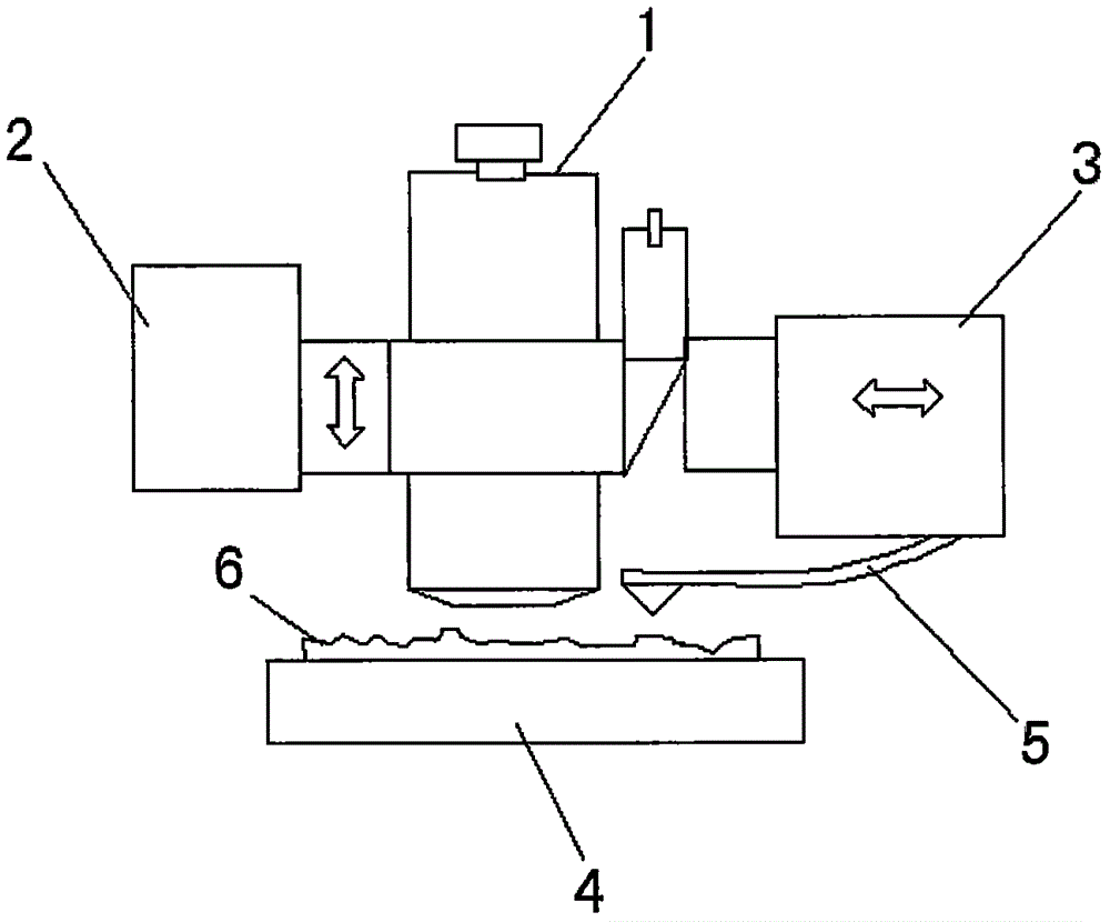
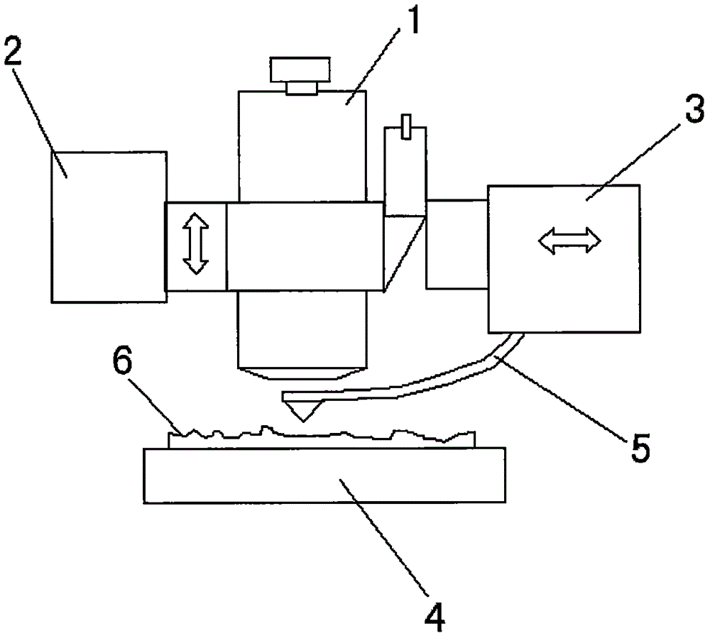
[0032] Such as Figure 1-2 As shown, the non-contact micro-nano three-dimensional measuring device described in the embodiment of the present invention includes a white light interference system 1, a probe sensing system, a Z-axis precision scanning system 2, a probe positioning system 3, an XY-axis precision scanning system 4, Control and data processing system; the Z-axis precision scanning system 2 is connected to the white light interference system 1, the white...


PUM


Abstract

The invention relates to a non-contact micro-nano three-dimensional measurement method, which measures the three-dimensional distribution of a sample in the white light interferometry mode; in the scanning probe precision measurement mode, uses scanning probe technology to combine white light interference and non-contact scanning probe The measurement technology is organically combined to finally realize the precise measurement of three-dimensional shape; non-contact micro-nano three-dimensional measurement device, including white light interference system, probe sensing system, Z-axis precision scanning system, probe positioning system, XY-axis precision scanning systems, control and data processing systems. The invention organically combines white light interference and non-contact scanning probe measurement technology, and can realize high-speed and high-precision three-dimensional shape measurement.

Description

technical field [0001] The invention belongs to the technical field of optical fine measurement, and in particular relates to a non-contact micro-nano three-dimensional measurement method and a device thereof. Background technique [0002] In recent years, the rapid development of IC equipment, semiconductor industry, and ultra-precision processing industry has put forward an urgent demand for high-precision measurement. Nanotechnology research is in full swing, MEMS technology has gradually entered the stage of industrialization from the laboratory, and there are signs of accelerated development in recent years. China is the largest consumer market for MEMS technology in the future, and the development of industrialization is imminent. There is an urgent market demand for high-precision micro-nano three-dimensional measuring instruments, especially for fast, high-precision, and real-time online detection instruments. [0003] Existing micro-nano measurement methods mainly ...

Claims


Application Information

Patent Timeline
IPC IPC(8): G01B11/24
CPCG01B11/24
Inventor 雷枫李少博问孝明
Owner 淮安普瑞精仪科技有限公司
Why Eureka
Try Eureka