
Vertical electrode structure of gallium nitride based light emitting diode
a technology of light-emitting diodes and vertical electrodes, which is applied in the manufacture of semiconductor/solid-state devices, electrical equipment, and semiconductor devices. it can solve the problems of short life, high manufacturing cost, and failure of present used traffic signals of lamps, so as to reduce the loss of fresnel refraction, facilitate reflection, and advance the effect of external luminous efficiency
- Summary
- Abstract
- Description
- Claims
- Application Information
AI Technical Summary
Benefits of technology
Problems solved by technology
Method used
Image

Examples
example 1
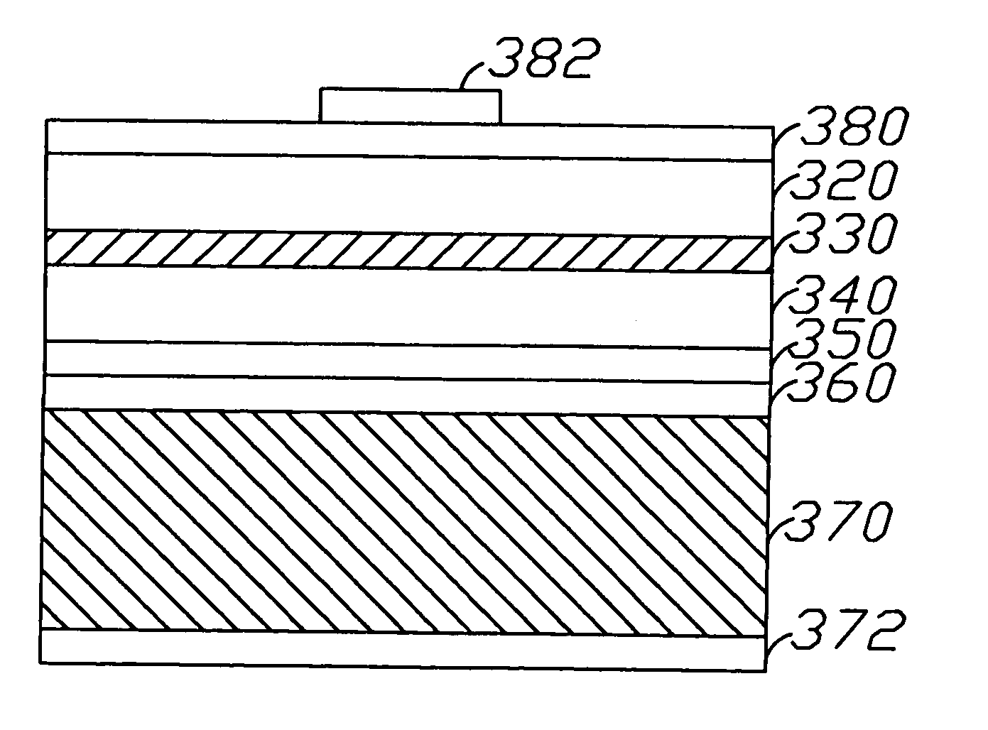
[0013] As shown in FIG. 3A, which is one of the embodiment of this invention, first of all, on a sapphire substrate 300, sequentially epitaxize a low temperature GaN buffer layer 310, a N-type AlInGaN ohmic contact layer 320, a AlInGaN light emitting layer 330, and a P-type AlInGaN ohmic contact layer 340. Following, a transparent ohmic contact metal layer 350 and a metal reflection layer 360 are subsequently formed on the P-type AlInGaN ohmic contact layer 340 by evaporating or sputtering technologies as shown in FIG. 3B. Then, the other conductive substrate 370 is bonded with the metal reflection layer 360 by thermal bonding as shown in FIG. 3C. Then, the FIG. 3D depicts that the sapphire substrate 10 is removed by laser liftoff or lapping technologies. And as shown in FIG. 3E, after laser liftoff, the remaining gallium metal on the surface of N-type AlInGaN ohmic contact layer 12 is removed by chemical etching to expose the N-type AlInGaN ohmic contact layer 320, and then, the N-...
example 2
[0014] As shown in FIG. 3A, which is another embodiment of this invention, first of all, on the sapphire substrate 300, sequentially epitaxize a low temperature GaN buffer layer 310, a N-type AlInGaN ohmic contact layer 320, a AlInGaN light emitting layer 330, and a P-type AlInGaN ohmic contact layer 340. Then a transparent ohmic contact metal layer 350 and a metal reflection layer 360 are subsequently formed on the P-type AlInGaN ohmic contact layer by evaporating or sputtering technologies as shown in FIG. 3B. As the depiction in FIG. 3C, another conductive substrate 370 is bonded with said metal reflection layer 360 by thermal bonding. Following, the sapphire substrate is removed by laser liftoff or lapping as shown in FIG. 3D. After laser liftoff, then, the remaining gallium metal on the surface of N-type AlInGaN ohmic contact layer 320 is eliminated by chemical etching to expose the N-type AlInGaN ohmic contact layer 320. Subsequently, the N-type transparent metal oxide layer 3...
example 3
[0015] As shown in FIG. 3A, which is another embodiment of the present invention, first of all, on the sapphire substrate 300, sequentially, epitaxize a low temperature GaN buffer layer 310, a N-type AlInGaN ohmic contact layer 320, a AlInGaN light emitting layer 330, and a P-type AlInGaN ohmic contact layer 340. Then a transparent ohmic contact metal layer 350 and a metal reflection layer 360 are subsequently formed on the P-type AlInGaN ohmic contact layer 340, as shown in FIG. 3B. Following, another conductive substrate 370 is bonded with said metal reflection layer 360 by thermal bonding as shown in FIG. 3C. Subsequently, the sapphire substrate 300 is removed by laser liftoff as the depiction in FIG. 3D. Then, the remaining gallium metal on the surface of the N-type AlInGaN ohmic contact layer 320 is eliminated by chemical etching to expose the N-type AlInGaN ohmic contact layer 320. And then the surface of N-type AlInGaN ohmic contact layer 320 is textured into a textured N-typ...
PUM
 Abstract
Description
Claims
Application Information