Semiconductor memory device

Inactive Publication Date: 2007-01-25
SEIKO EPSON CORP
View PDF4 Cites 0 Cited by
  • Summary
  • Abstract
  • Description
  • Claims
  • Application Information

AI Technical Summary

Benefits of technology

[0005] The present invention is to address the issues described above, and the object thereof is to achieve a reduction in the time required for writing data in a semiconductor memory device, and to achieve a reduction in the circuit structure required for specifying addresses.
[0007] Given the semiconductor memory device according to the first aspect of the present invention, an address counter having different maximum counter values at the time of reading data than at the time of writing data is used to specify the target address that is to be accessed, thus making it possible to both achieve a reduction in the data read time, and to achieve a reduction in the circuit structure required for specifying the address.
[0010] In the semiconductor memory device according to the first aspect of the present invention, the memory array is provided with a first memory area having a first ending address, and a second memory area, having a second ending address, and following the first memory area, where the maximum counter value at the time of writing is a counter value corresponding to the first ending address, and the maximum counter value at the time of reading may be a value wherein a specific value is added to the counter value corresponding to the second ending address. In this case, because the address specification process is not performed for the second storage area when writing data, it is possible to reduce the time required for writing data to the first storage area.

Problems solved by technology

However, sequential access semiconductor devices, when provided with a single data storage area that has an area that can be written that is smaller than the read-only area cannot return to the starting address of the writeable area without counting up until the final address of the read-only area first.
The result is a problem in that more time is required in the data writing process than in reading out data.

Method used


Image

  • Semiconductor memory device
  • Semiconductor memory device
  • Semiconductor memory device

Examples


Embodiment Construction

[0025] The semiconductor memory device according to the present invention, and the address control method in the semiconductor memory device, will be explained below based on example of embodiment, while referencing the figures.

Structure of the Semiconductor Memory Device

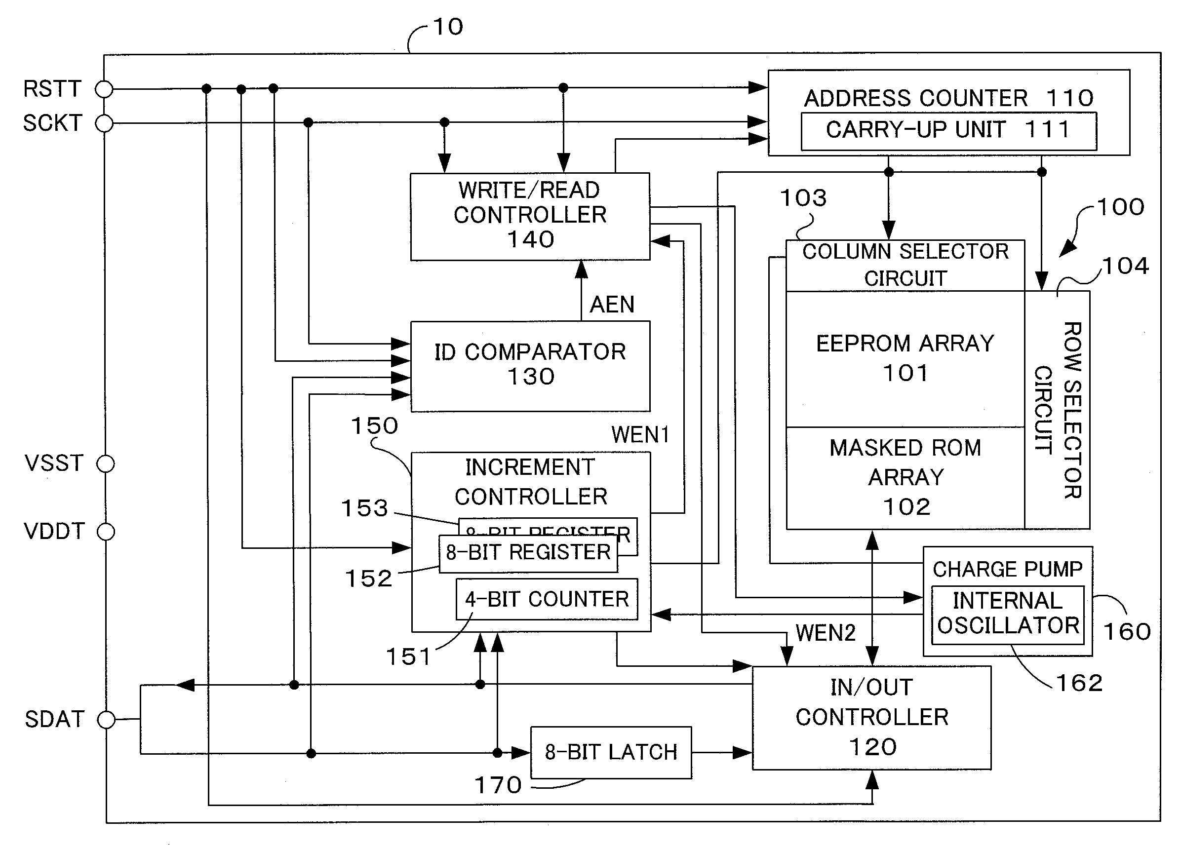
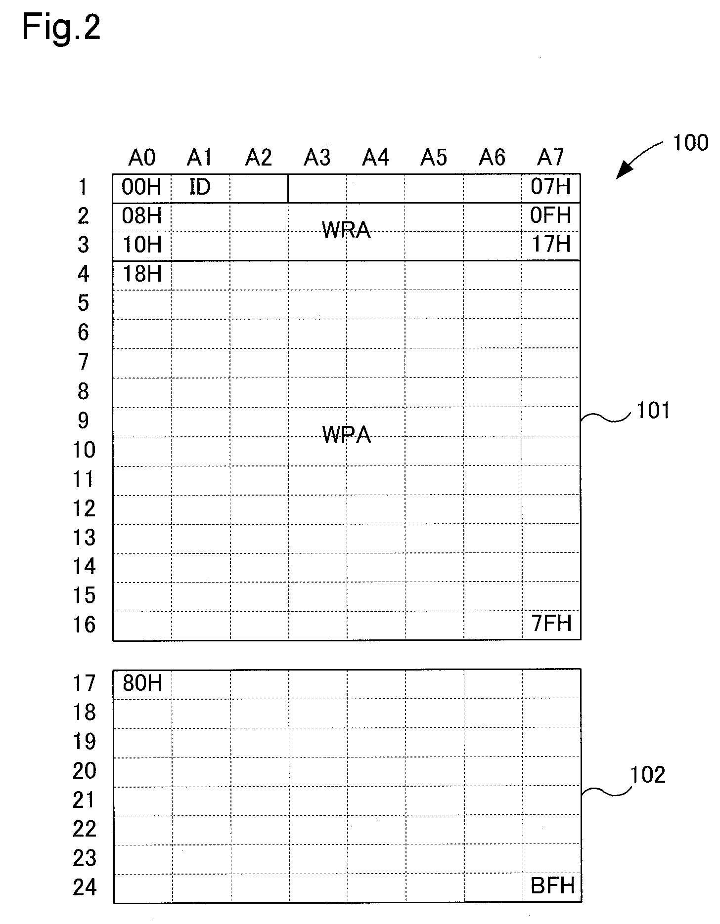
[0026] The structure of the semiconductor memory device 4 according to the present example of embodiment will be described in reference to FIG. 1 and FIG. 2. FIG. 1 is a block diagram illustrating the functional internal structure of a semiconductor memory device according to the present example of embodiment. FIG. 2 is an explanatory diagram illustrating schematically an internal structural map of a memory array provided in the semiconductor memory device according to the present example of embodiment.

[0027] In the present example of embodiment, a semiconductor memory device 10 is a sequential access-type memory device that does not require the inputting of address data from the outside to specify the address f...


PUM


Abstract

In a semiconductor memory device 10, the maximum counter value in a carry-up unit 111 of an address counter 110 is set to 128 bits when an access request is for writing data to a memory array 100. On the other hand, in the semiconductor memory device 10, if the access request is for reading data from the memory array 100, the maximum counter value in the carry-up unit 111 of the address counter 110 is set to 256 bits. The result is that it is possible to reduce the circuit structure required for specifying the desired address in an EEPROM array 101 and a masked ROM array 102.

Description

FIELD OF TECHNOLOGY [0001] The present invention relates to semiconductor memory devices accessed sequentially, and to address control methods in semiconductor memory devices that are accessed sequentially. BACKGROUND ART [0002] EEPROMs are known as semiconductor memory devices wherein the data cells in the memory array can only be accessed sequentially. Because this type of semiconductor memory device is relatively inexpensive, it is used as a memory device for storing data pertaining to the quantity of remaining consumable materials or the quantity of consumable materials used. Moreover, there are also semiconductor memory devices that have been produced that have multiple data storage areas, for example, EEPROM areas and masked ROM areas. In semiconductor memory devices that have multiple data storage areas, the use of masked ROM area has the benefit of eliminating the need for writing read-only data to the semiconductor memory device. [0003] However, sequential access semiconduc...

Claims


Application Information

Patent Timeline
IPC IPC(8): G11C8/00
CPCG11C16/08G11C8/04G11C8/00
Inventor ASAUCHI, NOBORU
Owner SEIKO EPSON CORP
Why Eureka
Try Eureka