Method and monitor structure for detecting and locating IC defects
a technology of ic defects and monitor structures, applied in semiconductor/solid-state device testing/measurement, semiconductor/solid-state device details, instruments, etc., can solve the problem that the underlying metallization layer cannot detect the presence of defects in the recent formation of metallization layers
- Summary
- Abstract
- Description
- Claims
- Application Information
AI Technical Summary
Benefits of technology
Problems solved by technology
Method used
Image

Examples
Embodiment Construction
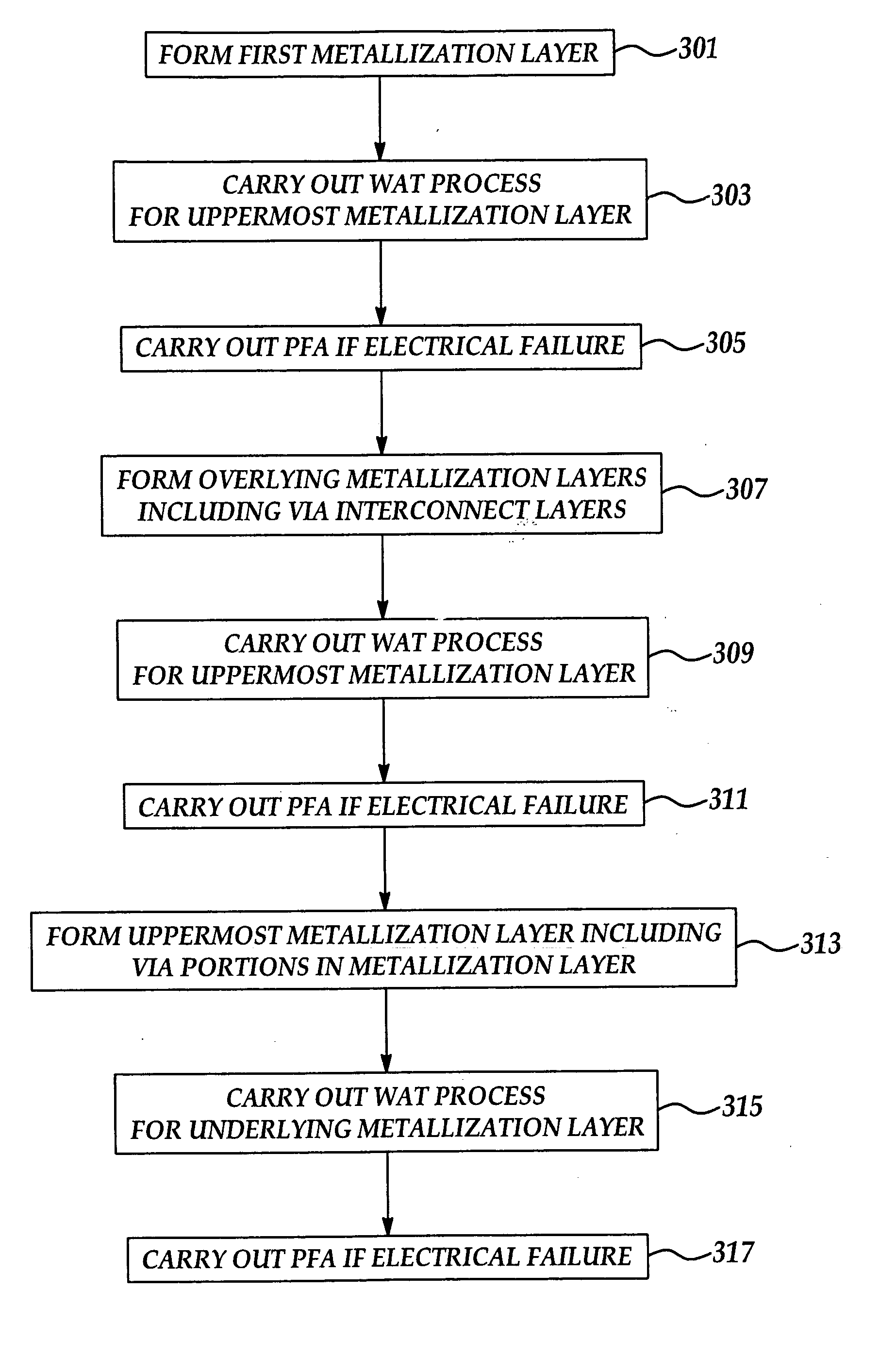
[0015] Although the method and apparatus of the present invention is explained and is particularly advantageous for determining the existence of and location of defects in copper or copper alloy metallization layers forming portions of a process control monitor for determining the reliability of an integrated circuit manufacturing process, it will be appreciated that other conductive materials including aluminum and tungsten may be used. Further although, the nature of underlying metallization layer metal interconnect defects are discussed with respect to via induced metal island corrosion (VIMIC) effects, it will be appreciated that the 3-dimentional metal interconnect process control monitor (PCM) structure including a method for detecting and locating metal interconnect defects may be applied, in general, to the detection and location of electrical continuity defects in underlying metallization layers.
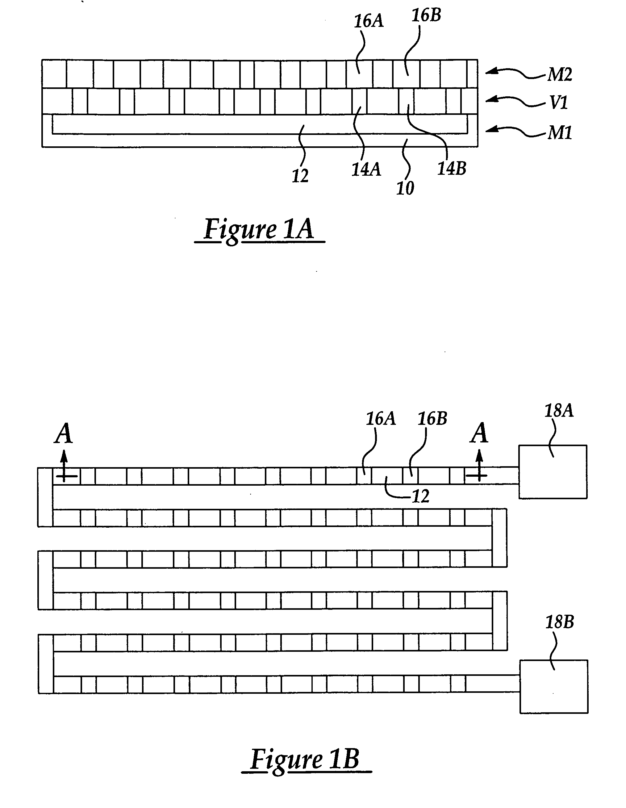
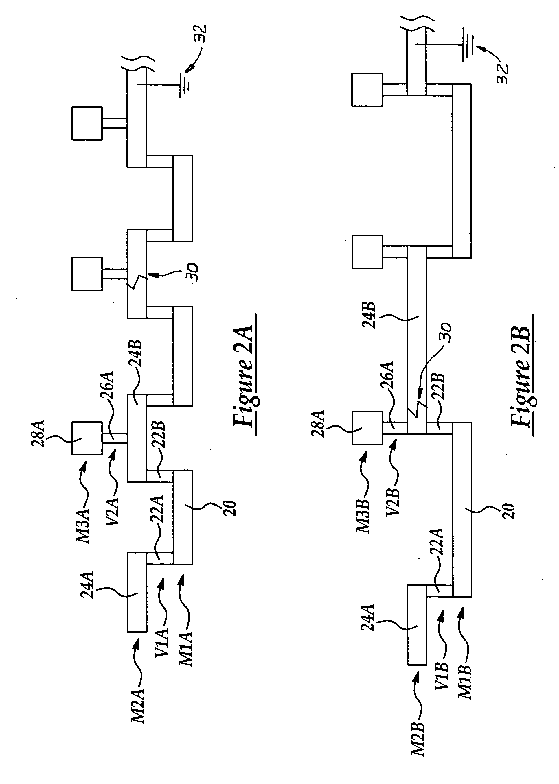
[0016] Referring to FIG. 1A is shown a cross sectional view of a portion of an...
PUM
 Abstract
Description
Claims
Application Information
 - R&D Engineer
- R&D Manager
- IP Professional
- Industry Leading Data Capabilities
- Powerful AI technology
- Patent DNA Extraction
Browse by: Latest US Patents, China's latest patents, Technical Efficacy Thesaurus, Application Domain, Technology Topic.
© 2024 PatSnap. All rights reserved.Legal|Privacy policy|Modern Slavery Act Transparency Statement|Sitemap