Printed wiring board and production method therefor

a printing method and wiring board technology, applied in the direction of printed circuit details, printed circuits, printed connections, etc., can solve the problems of reducing the reliability of via holes on connectability, difficulty in forming finer wiring patterns on thicker conductive layers, and thin printed wiring boards with lower stiffness. , to achieve the effect of sufficient adhesiveness and high stiffness

Inactive Publication Date: 2007-02-01
MEIKO ELECTRONICS CO LTD
View PDF3 Cites 21 Cited by
  • Summary
  • Abstract
  • Description
  • Claims
  • Application Information

AI Technical Summary

Benefits of technology

[0020] A purpose of the present invention is to provide a printed wiring board, for example, a multilayer build-up printed wiring board, that exhibits higher stiffness and more sufficient adhesiveness between a wiring layer and an insulating layer, whereas having finer wiring patterns, and also a method producing such a printed wiring board, employing subtractive etching or semi-additive processing.

Problems solved by technology

Generally, thinner printed wiring boards suffer from lower stiffness.
It is also well known that subtractive etching causes difficulty in forming a finer wiring pattern on a thicker conductive layer.
The method disclosed in the document 2, however, could lower the reliability of via holes on connectability.
However, it is a well known fact that such a process cannot give sufficient adhesiveness to the interface of a plated layer and an insulating layer.

Method used


Image

  • Printed wiring board and production method therefor
  • Printed wiring board and production method therefor
  • Printed wiring board and production method therefor

Examples


first embodiment

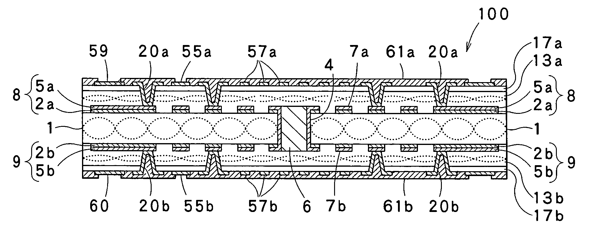
[0051] Disclosed first with reference to FIGS. 1 to 10 is a first embodiment of a method of producing a printed wiring board, according to the present invention, employing subtractive etching. An exemplary printed wiring board to be produced in the first embodiment is a four-layer printed wiring board.

[0052] A feature of the first embodiment is to provide insulating layers with a dual-layer construction that consists of a first insulating layer formed by curing a B-staged insulative sheet made of a high-stiff sheet-type reinforcing material containing resin and a second insulating layer formed by curing resin ink containing particles or components soluble to an agent such as an oxidant or an acid, or a first insulating layer for higher stiffness and a second insulating layer for higher adhesiveness.

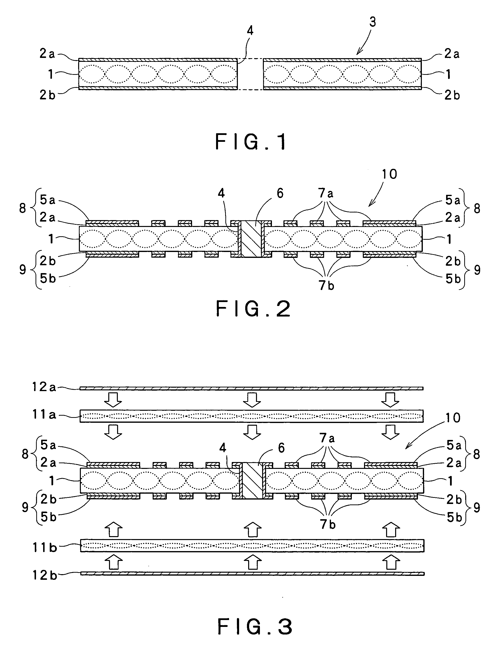
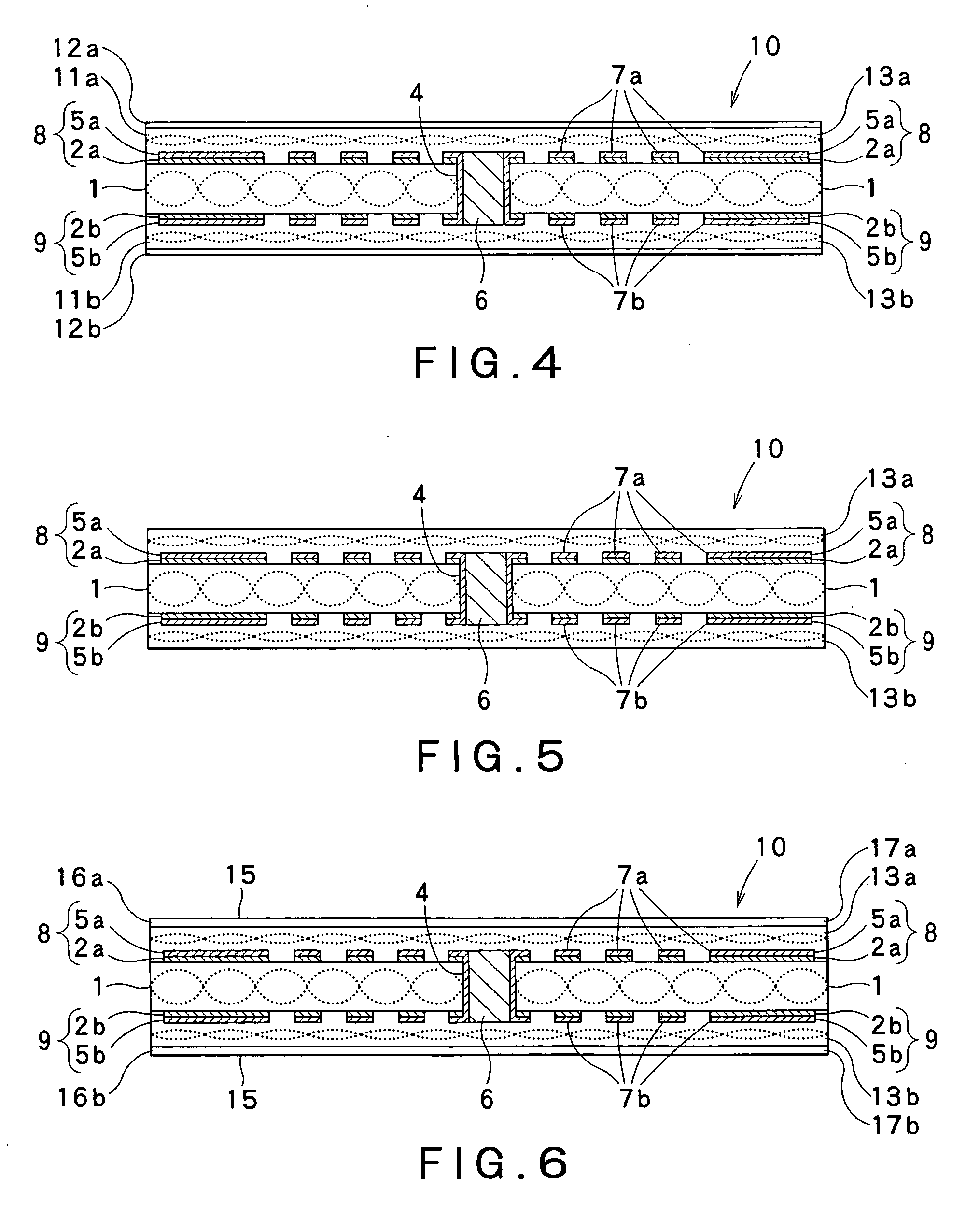
[0053] (Processing Step A1)

[0054] A processing step A1 is described with reference to FIG. 1.

[0055] Prepared first is a double-sided copper-coated board 3. The board 3 is made of a co...

second embodiment

[0110] Disclosed next with reference to FIGS. 8 and 11 to 16 is a second embodiment of a method of producing a printed wiring board, according to the present invention, employing semi-additive processing. An exemplary printed wiring board to be produced in the second embodiment is also a four-layer printed wiring board.

[0111] Different from the first embodiment employing subtractive etching, the second embodiment employs semi-additive processing. In general, semi-additive processing requires a higher number of processing steps than subtractive etching, however, more advantageous on achieving finer and denser wiring patterns.

[0112] The second embodiment is identical to the first embodiment, except for a wiring pattern forming process. The elements in the second embodiment that are the same as or analogous to those in the first embodiment are given the same reference numerals as those in the first embodiment, and not described in detail or the description thereof is omitted.

[0113] ...

third embodiment

[0135] Disclosed next with reference to FIGS. 17 to 23 is a third embodiment of a method of producing a printed wiring board, according to the present invention, employing subtractive etching, that gives further advantages to the first and second embodiments.

[0136] In detail, the third embodiment achieves finer and denser wiring patterns not only on the third and fourth wiring layers 23 and 24 (the first embodiment) or the third and fourth wiring layers 59 and 60 (the second embodiment), but also the first and second wiring layers 8 and 9, in a four-layer printed wiring board.

[0137] The elements in third embodiment that are the same as or analogous to those in the first embodiment are given the same reference numerals as those in the first embodiment, and not described in detail or the description thereof is omitted.

[0138] (Processing Step C1)

[0139] A processing step C1 is described with reference to FIGS. 17 and 18.

[0140] Prepared first is a double-sided copper-coated board 3 ...


PUM


Abstract

A printed wiring board has a first wiring layer formed at least on one surface of an insulative substrate, an insulating layer formed as covering the first wiring layer, and a second wiring layer formed on the insulating layer. The insulating layer is formed of a cured insulative sheet made of a high-stiff sheet-type reinforcing material containing resin. The first and second wiring layers are electrically connected to each other through at least one hole having a bottom. The second wiring layer is united with the insulating layer at an interface thereof with a conductive material of the second wiring layer injected into concave sections provided on the interface. Another printed wiring board has an insulative substrate having a first surface and a second surface, a first insulating layer and a second insulating layer formed on the first surface and the second surface, respectively, and a first wiring layer formed on the first insulating layer and a second wiring layer formed on the second insulating layer. The first and second wiring layers are electrically connected to each other via at least one through hole. The first wiring layer is united with the first insulating layer at an interface thereof with a conductive material of the first wiring layer injected into concave sections provided on the interface. The second wiring layer is united with the second insulating layer at an interface thereof with a conductive material of the first wiring layer injected into concave sections provided on the interface.

Description

CROSS-REFERENCE TO RELATED APPLICATIONS [0001] This application is based on and claims the benefit of priority from the prior Japanese Patent Application No. 2005-221702 filed on Jul. 29, 2005, the entire contents of which are incorporated herein by reference. BACKGROUND OF THE INVENTION [0002] The present invention relates to a printed wiring board and a method producing such a printed circuit. [0003] Known printed wiring boards are produced by a method, for example, disclosed in Japanese Unexamined Patent Publication No. 2005-86164 (referred to as document 1, hereinafter). [0004] The method disclosed in the document 1 is as follows: Prepared is a core substrate containing glass cloth. First and second wiring layers are formed on both sides of the core substrate and connected to each other through interstitial via holes (IVH). A B-staged insulative sheet containing glass cloth and copper foil are placed in this order on each wiring layer and laminated by thermal press. The laminate...

Claims


Application Information

Patent Timeline
Patent Type & Authority Applications(United States)
IPC IPC(8): H05K1/00
CPCH05K3/387H05K3/4661H05K2201/0209H05K2201/0212H05K2203/1152H05K2203/0773H05K2203/0789H05K2203/0796H05K2201/09518
Inventor SHIMADA, HIROSHIMICHIWAKI, SHIGERUSHISHIME, KAZUO
Owner MEIKO ELECTRONICS CO LTD
Why Eureka
Try Eureka