

Semiconductor integrated circuit device
a technology of integrated circuits and semiconductors, applied in error detection/correction, digital storage, instruments, etc., can solve the problems of ecc operation, large power consumption, and inability to access,
- Summary
- Abstract
- Description
- Claims
- Application Information
AI Technical Summary
Problems solved by technology
Method used
Image


Examples
first embodiment
(First Embodiment)
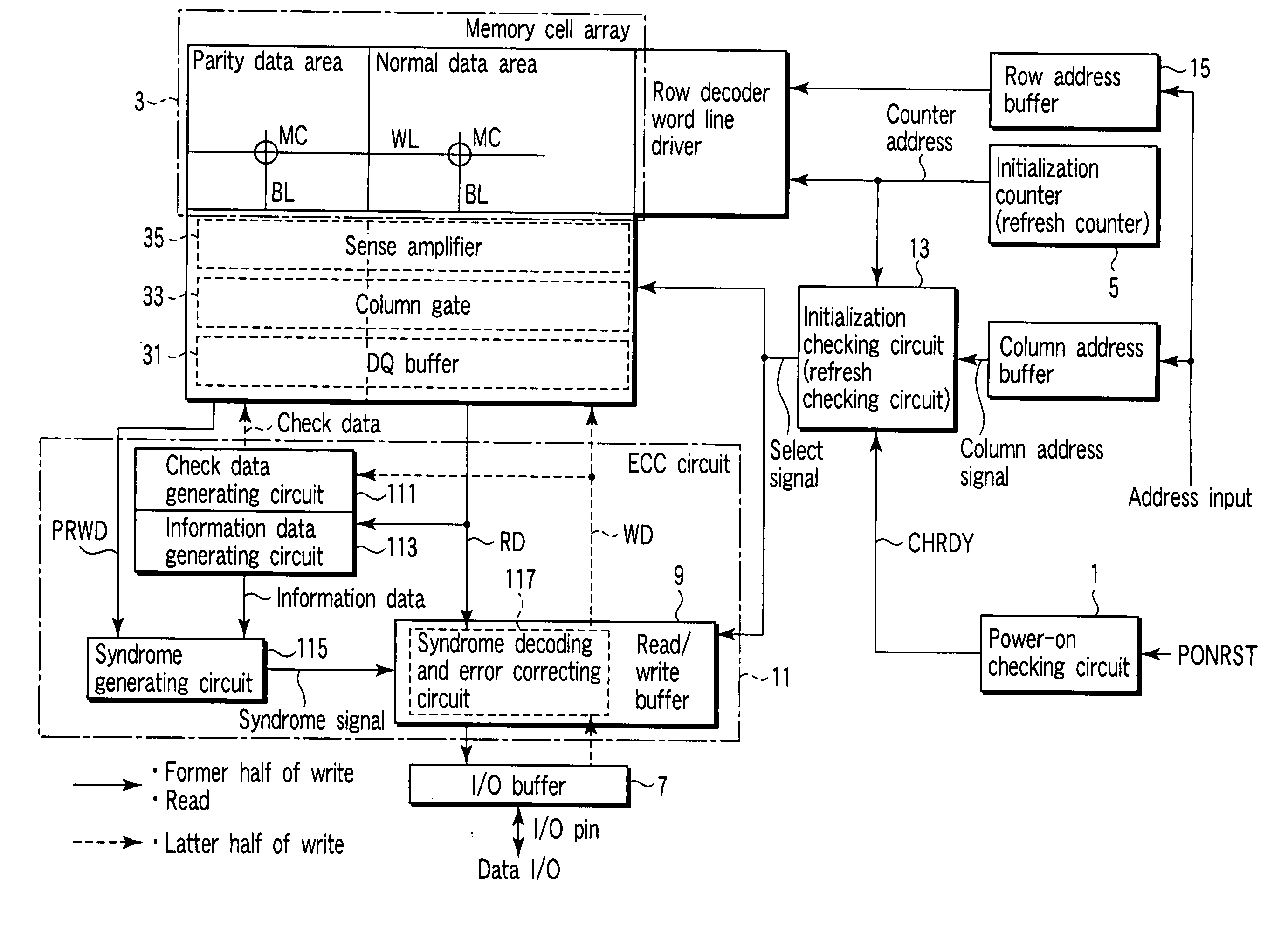
[0034]FIG. 1 is a block diagram showing the exemplary configuration of a semiconductor integrated circuit device according to a first embodiment of the present invention.
[0035] As shown in FIG. 1, the semiconductor integrated circuit device according to the first embodiment comprises a power-on checking circuit 1, a memory cell array 3, an initialization counter 5, an I / O buffer (I / O buffer) 7, a read / write buffer 9, an error checking and correcting circuit 11, and an initialization checking circuit 13.
[0036] The power-on checking circuit 1 detects power-on. The power-on checking circuit in the present example detects power-on when a power-on reset signal is input, and outputs a power-on checking signal CHARY that activates the integrated circuit device.
[0037] Memory cells are integrated in the memory cell array 3. The memory cell array 3 in the present example has a normal data area and a parity data area. Normal data is stored in the normal data area. Check da...
second embodiment
(Second Embodiment)
[0093]FIG. 11 is a block diagram showing the exemplary configuration of a semiconductor integrated circuit device according to a second embodiment of the present invention.
[0094] As shown in FIG. 11, the second embodiment differs from the first embodiment in that the initialization detecting circuit (refresh checking circuit) 13-2 references not only the counter address but also an error monitor signal indicating whether or not an error has occurred, in outputting the select signal. The other arrangements of the second embodiment are similar to those of the first embodiment.
[0095] The error monitor signal is generated by an error monitor signal generating circuit 201. The error monitor signal generating circuit 201 in. the present example generates an error monitor signal with reference to the syndrome signal. The error monitor signal generating circuit 201 in the present example is reset upon detecting an address transition checking signal ATD. Specifically, th...
third embodiment
(Third Embodiment)
[0114]FIG. 16 is a flowchart showing the exemplary operational flow of a semiconductor integrated circuit device according to a third embodiment of the invention.
[0115] As shown in FIG. 16, the operational flow of the third embodiment is similar to that of the first embodiment except for a procedure executed after the determination of whether or not all the memory cells have been refreshed as shown in ST. 2, particularly a procedure executed if not all the memory cells have been refreshed (No).
[0116] In the third embodiment, if not all the memory cells have been refreshed (No), the device determines whether or not an error is detected in the M×N-bit normal data (RD) read from the normal data area (ST. 3).
[0117] If no error is detected in the normal data (No), only the N-bit write data of the M×N-bit normal data (WD) is written to the normal data area of the memory cell array 3 (ST. 4). This operation is similar to that shown in FIG. 8 in the first embodiment.
[0...
PUM
 Abstract
Description
Claims
Application Information