Semiconductor integrated circuit

Active Publication Date: 2007-04-12
CETUS TECH INC
View PDF13 Cites 2 Cited by
  • Summary
  • Abstract
  • Description
  • Claims
  • Application Information

AI Technical Summary

Benefits of technology

[0006] An object of the present invention is providing a dynamic semiconductor integrated circuit capable of achieving both speedup and malfunction protection during low-voltage operation.
[0008] With the configuration described above, the fourth transistor permits conduction between the first power supply and the output node even after the second and third transistors are turned ON. Hence, occurrence of a glitch at the output node can be suppressed, and thus occurrence of a malfunction can be prevented. Also, once being turned OFF, the fourth transistor does not permit conduction between the first power supply and the output node, letting the output node change its potential. Hence, the operation speed is prevented from decreasing even during low-voltage operation.
[0011] According to the present invention, both speedup and malfunction protection can be achieved even when the power supply voltage is low, and thus the range of the power supply voltage with which the circuit is operable can be widened.

Problems solved by technology

Also, once being turned OFF, the fourth transistor does not permit conduction between the first power supply and the output node, letting the output node change its potential.

Method used


Image

  • Semiconductor integrated circuit
  • Semiconductor integrated circuit
  • Semiconductor integrated circuit

Examples


Embodiment Construction

[0025] Hereinafter, preferred embodiments of the present invention will be described with reference to the accompanying drawings.

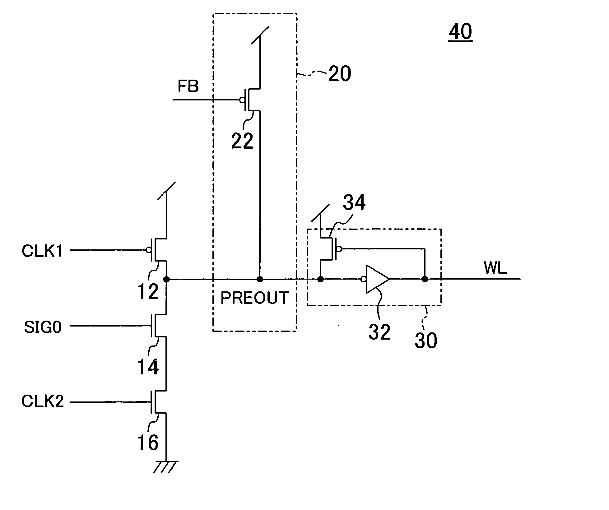
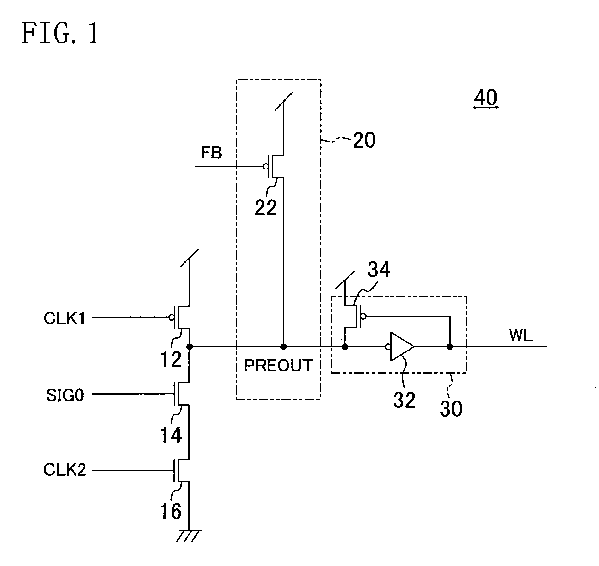
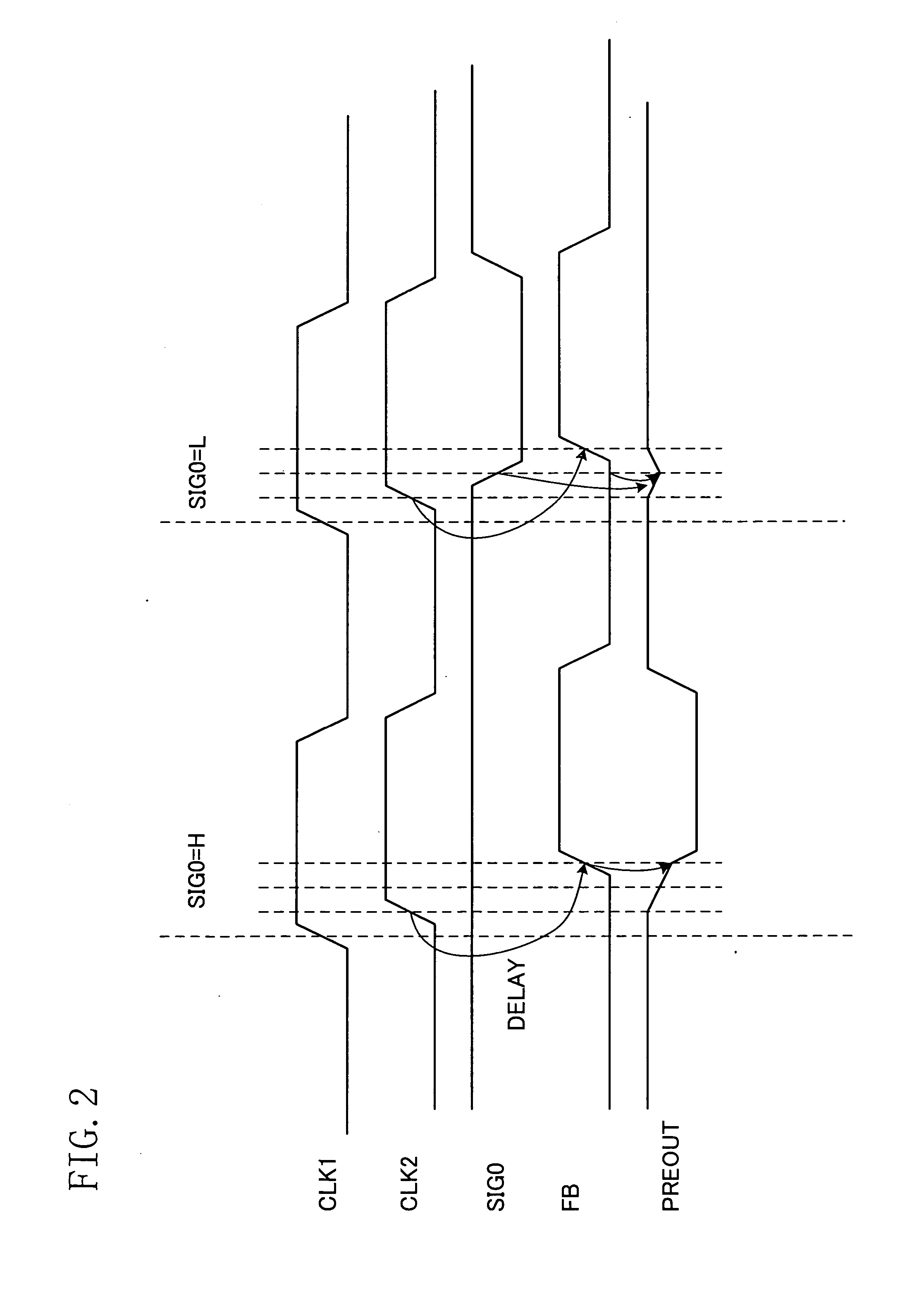
[0026]FIG. 1 is a circuit diagram of a semiconductor integrated circuit of an embodiment of the present invention. The semiconductor integrated circuit of FIG. 1, denoted by 40, includes a PMOS transistor 12, NMOS transistors 14 and 16, a feedback circuit 20 and a hold circuit 30, constituting as a whole a dynamic circuit. The feedback circuit 20 includes a PMOS transistor 22, and the hold circuit 30 includes an inverter 32 and a PMOS transistor 34.

[0027] Clocks CLK1 and CLK2 are respectively input into the gates of the PMOS transistor 12 and the NMOS transistor 16. The clock CLK2 is synchronous with the clock CLK1. A signal SIG0 is input into the gate of the NMOS transistor 14. The NMOS transistors 14 and 16 are connected in series.

[0028] A feedback signal FB is input into the gate of the PMOS transistor 22. The feedback signal FB is a signal that shif...


PUM


Abstract

The semiconductor integrated circuit includes: a first transistor of a first conductivity type connected between a first power supply and an output node and turned ON according to a first clock to put the output node to a first logic level; a second transistor of a second conductivity type turned ON according to an input signal; a third transistor of the second conductivity type connected in series to the second transistor and turned ON according to a second clock; and a fourth transistor of the first conductivity type connected between the first power supply and the output node and turned ON according to a feedback signal. The second and third transistors are connected between the output node and a second power supply. The fourth transistor is turned from ON to OFF after both the second and third transistors are turned ON.

Description

BACKGROUND OF THE INVENTION [0001] The present invention relates to a dynamic semiconductor integrated circuit, and more particularly, to achievement of speedup and malfunction protection during low-voltage operation. [0002] Dynamic circuits are used for circuits requiring high-speed operation such as memory circuits. Use of static circuits for such circuits will increase the gate capacitance preventing high-speed operation. [0003] A semiconductor integrated circuit using a dynamic circuit is disclosed in Japanese Laid-Open Patent Publication No. 2003-318727. The disclosed circuit is provided with a hold circuit having an inverter and a p-channel metal oxide semiconductor (PMOS) transistor for protection against a malfunction. The input terminal of the inverter is connected to an output node, the gate of the PMOS transistor is connected to the output of the inverter, and the drain of the PMOS transistor is connected to the output node, so that the PMOS transistor can supply charge t...

Claims


Application Information

Patent Timeline
IPC IPC(8): H03K19/096
CPCH03K19/01855H03K19/0963
Inventor MASUO, AKIRASUMITANI, NORIHIKO
Owner CETUS TECH INC
Why Eureka
Try Eureka