Gas supply device and apparatus for processing a substrate

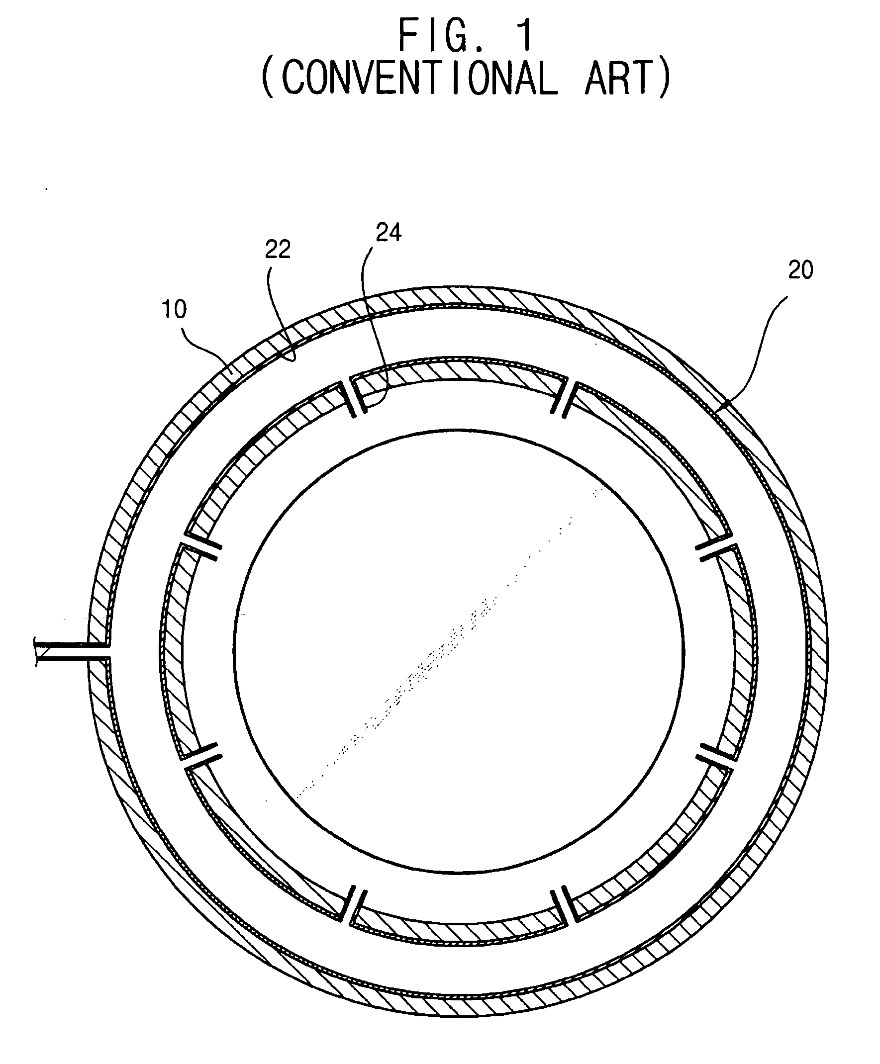
a gas supply device and substrate technology, applied in lighting and heating apparatus, combustion types, combustion using lumps and pulverizing fuels, etc., can solve problems such as poor uniformity of the pattern formed on the substrate by etching the layer, and the inability to uniformly spray the processing gas from the nozzle,

Inactive Publication Date: 2007-04-19
SAMSUNG ELECTRONICS CO LTD
View PDF3 Cites 277 Cited by
  • Summary
  • Abstract
  • Description
  • Claims
  • Application Information

AI Technical Summary

Problems solved by technology

However, the processing gas may not be uniformly sprayed from the nozzles 24 onto the substrate.
Additionally, if an etching gas is provided from the nozzles 24, a pattern that may be formed on the substrate by etching the layer may have a poor uniformity.
For example, this problem may become more serious if a semiconductor device has a minute design rule and / or if a semiconductor substrate has an increased size.

Method used


Image

  • Gas supply device and apparatus for processing a substrate
  • Gas supply device and apparatus for processing a substrate
  • Gas supply device and apparatus for processing a substrate

Examples


Embodiment Construction

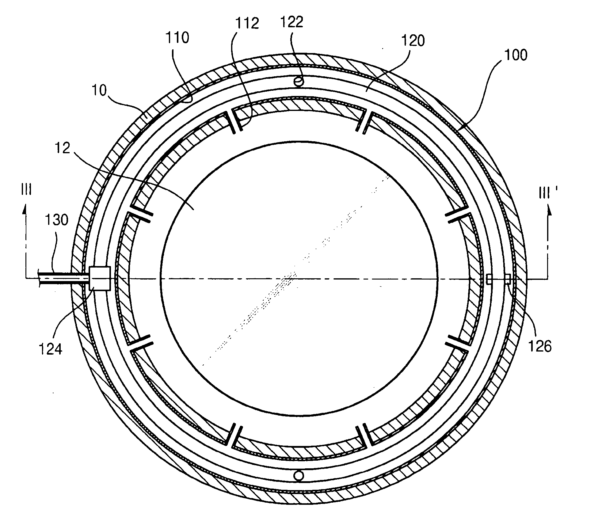
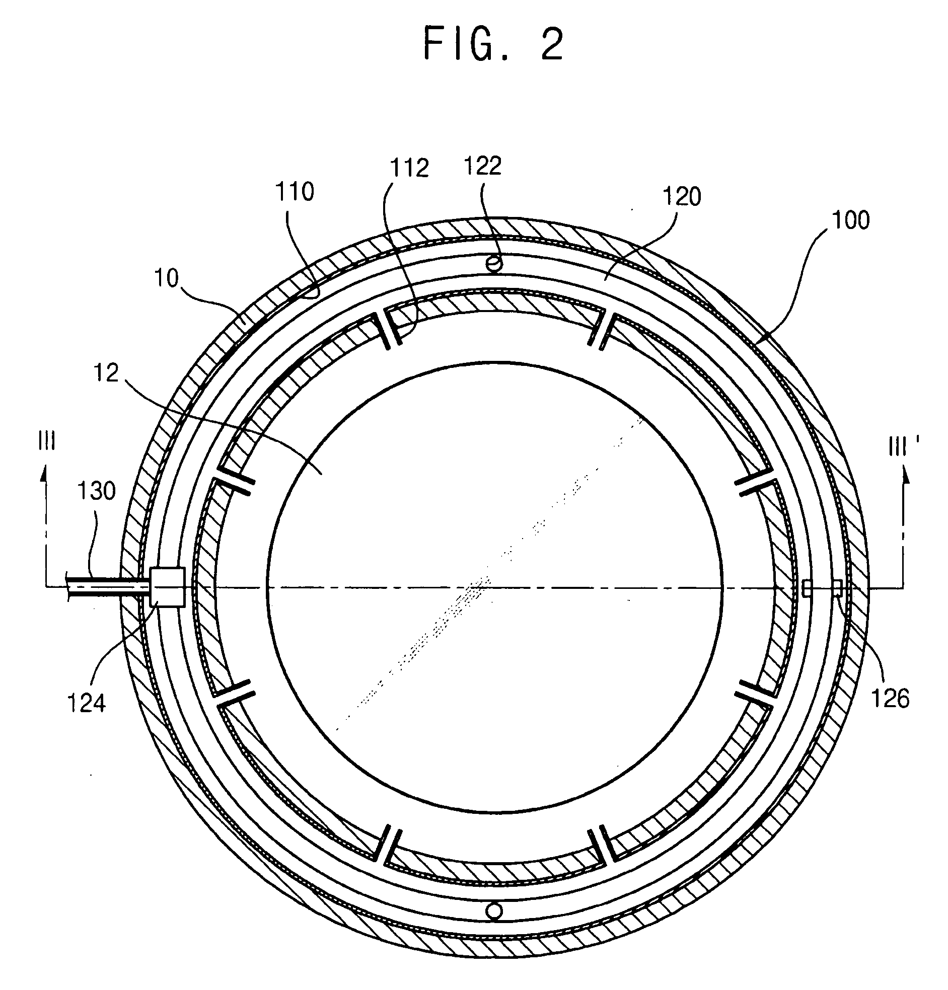
[0043] Various example, non-limiting embodiments will now be described more fully with reference to the accompanying drawings. Example embodiments may, however, be in many different forms and should not be construed as limited to the example embodiments set forth herein. Accordingly, these example, non-limiting embodiments are provided so that this disclosure will be thorough and complete, and will fully convey the scope to those skilled in the art. In the drawings, the sizes and relative sizes of the features and elements may be exaggerated for clarity.

[0044] It will be understood that when a feature or an element is referred to as being “on,”“connected to” or “coupled to” another feature or element, it can be directly on, connected or coupled to the other feature or element or intervening features or elements that may be present. In contrast, when an element is referred to as being “directly on,”“directly connected to” or “directly coupled to” another feature or element, there ar...


PUM

PropertyMeasurementUnit
angleaaaaaaaaaa
angleaaaaaaaaaa
internal pressureaaaaaaaaaa

Abstract

A gas supply device may include a first gas supply member that may be disposed in a chamber and around a substrate loaded in the chamber. The first gas supply member may include nozzles for providing a gas onto the substrate. A second gas supply member that may provide the gas supplied from at least one gas supply line to the first gas supply member.

Description

PRIORITY STATEMENT [0001] This U.S. non-provisional application claims benefit of priority under 35 U.S.C. § 119 from Korean Patent Application No. 2005-97979 filed on Oct. 18, 2005 in the Korean Intellectual Property Office (KIPO), the entire contents of which are incorporated herein by reference. BACKGROUND [0002] 1. Field [0003] Example embodiments relate to a gas supply device and an apparatus for processing a substrate having the gas supply device, for example, a gas supply device for supplying a reaction gas onto a substrate. [0004] 2. Description of the Related Art [0005] A semiconductor manufacturing process may include a fabrication process, an electrical die sorting (EDS) process and / or a packaging process. Integrated circuits including various elements may be formed on a silicon wafer in the fabrication process. Electrical characteristics of the integrated circuits may be inspected in the EDS process. The integrated circuits may be sealed and separated individually in the...

Claims


Application Information

Patent Timeline
Patent Type & Authority Applications(United States)
IPC IPC(8): F23C5/08
CPCC23C16/45508C23C16/4558H01L21/02
Inventor KIM, WOO-SEOKHAN, JAE-HYUNHONG, JOO-PYOHUH, NO-HYUN
Owner SAMSUNG ELECTRONICS CO LTD
Why Eureka
Try Eureka