Electrostatic discharge protection structure and thin film transistor substrate including the same

Inactive Publication Date: 2007-04-26
CHUNGHWA PICTURE TUBES LTD
View PDF8 Cites 28 Cited by
  • Summary
  • Abstract
  • Description
  • Claims
  • Application Information

AI Technical Summary

Benefits of technology

[0014] The ESD protection structure according to the present invention has a floating conductive pattern crossing over a conducting wire on the space-limited substrate, thereby to introduce electrostatic energy to the floating conductive pattern for energy dis

Problems solved by technology

In the manufacture of thin film transistor liquid crystal display devices (TFT-LCDs), electrostatic discharge (ESD) protection has been an important issue.
Otherwise, the electrostatic charge accumulating to a specific amount will be discharged through any place on the substrate, thus impairing a part of the pixel structure, resulting in display defects or even damage of the whole display device.
The space is not available for the outer short ring in COG technique du

Method used


Image

  • Electrostatic discharge protection structure and thin film transistor substrate including the same
  • Electrostatic discharge protection structure and thin film transistor substrate including the same
  • Electrostatic discharge protection structure and thin film transistor substrate including the same

Examples


Example

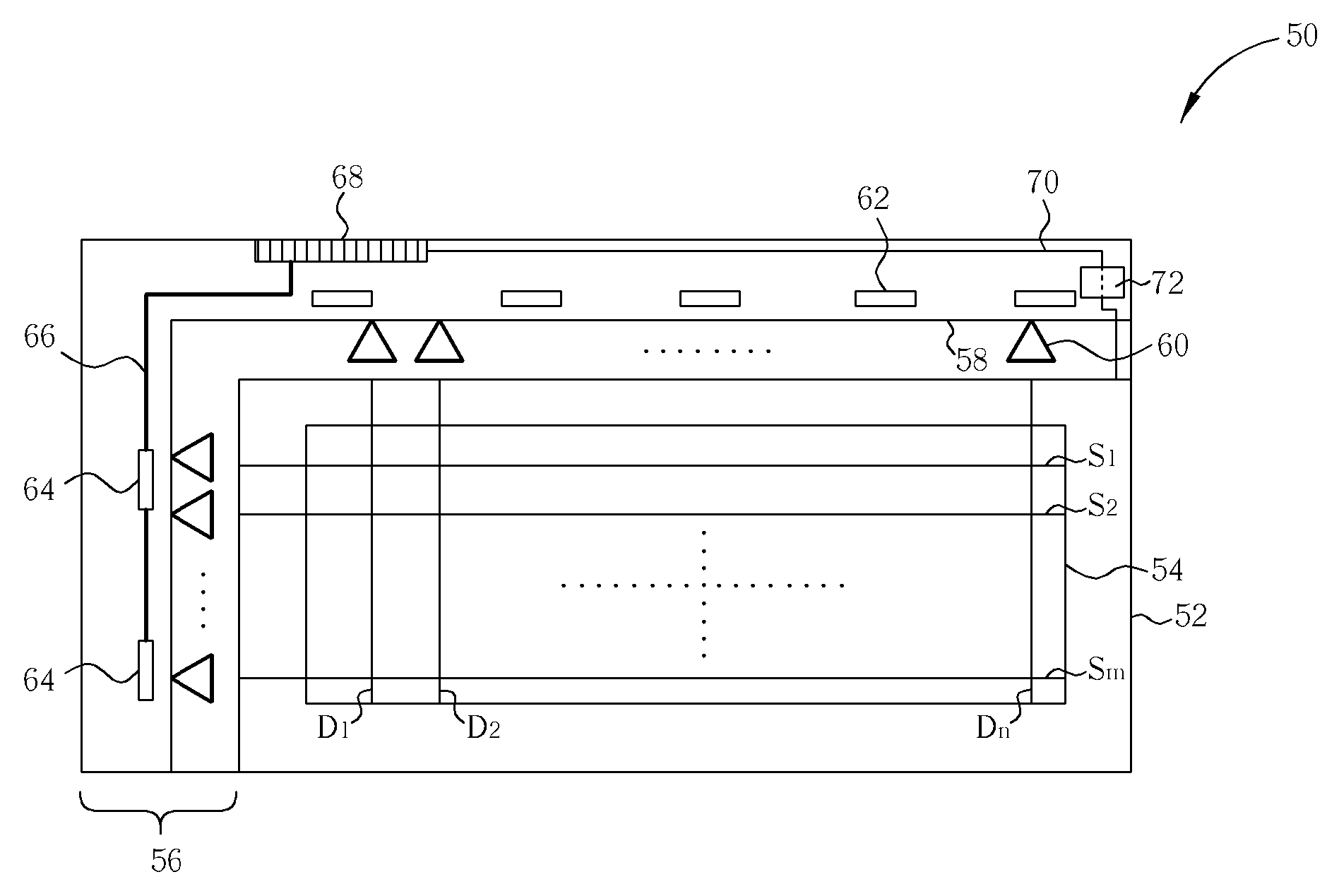
[0021] Please refer to FIG. 3. FIG. 3 is a schematic diagram showing a TFT substrate structure having an ESD protection structure according to the present invention. Each drawing herein is a schematic drawing and thus the size of each element is not to scale. As shown in FIG. 3, a TFT substrate 50 comprises a transparent insulating substrate 52, a plurality of source driver IC chips 62, and a plurality of gate driver IC chips 64. A plurality of scan lines S1, S2, . . . , and Sm and a plurality of data lines D1, D2, . . . , and Dn are positioned on the transparent insulting substrate 52. The scan lines S1, S2, . . . , and Sm orthogonally cross over the data lines D1, D2, . . . , and Dn to define a pixel matrix and pixel electrodes (not shown) are disposed. The source driver IC chip 62 and the gate driver IC chips 64 are disposed in the OLB region 56 on the transparent insulating substrate 52 for outputting image data signals to the data lines D1, D2, . . . , and Dn and outputting swi...


PUM


Abstract

An electrostatic discharge protection structure contains a short ring surrounding a display region comprising pixel electrodes and thin film transistors, a plurality of switching elements disposed between the display region and the short ring corresponding to the scan lines and data lines, at least one of which is turned on to electrically connect the short ring and the scan lines and the data lines for introducing electrostatic charges to the short ring when a specific amount of electrostatic charges accumulate on the scan lines and the data lines, a conducting wire electrically connecting a storage capacitor line and the short ring, and a floating conductive pattern crossing over and not contacting the conducting wire, thereby assisting the electrostatic charges in distributing in the floating conductive pattern. Thus, an electrostatic discharge protection can be performed efficiently without increasing the substrate size.

Description

BACKGROUND OF THE INVENTION [0001] 1. Field of the Invention [0002] The present invention relates to an electrostatic discharge protection structure, and particularly to an electrostatic discharge protection structure used in a thin film transistor substrate, the thin film transistor substrate comprising the electrostatic discharge protection structure. [0003] 2. Description of the Prior Art [0004] In the manufacture of thin film transistor liquid crystal display devices (TFT-LCDs), electrostatic discharge (ESD) protection has been an important issue. There would be a lot of electrostatic charges accumulating on the surface of the substrate of the display during a series of manufacturing processes, such as, dry etching, and a combination of a TFT substrate and a color filter (CF) substrate, and delivery of the substrate, unless there is a proper way to discharge the charges. Otherwise, the electrostatic charge accumulating to a specific amount will be discharged through any place on...

Claims


Application Information

Patent Timeline
IPC IPC(8): G02F1/1333
CPCG02F1/13454G02F1/136204
Inventor HUANG, CHIN-HAIYU, HONG-TIANSHIAU, FU-YUAN
Owner CHUNGHWA PICTURE TUBES LTD
Why Eureka
Try Eureka