Semiconductor laser element and method of fabrication thereof

a technology of semiconductor laser elements and laser elements, which is applied in the direction of laser cooling arrangements, laser details, semiconductor lasers, etc., can solve the problems of high element resistance, high operational voltage of semiconductor laser elements, complicated fabrication processes, etc., and achieves convenient ridge formation, sufficient etching selectivity, and the effect of forming a semiconductor laser element stacked structure in a short tim

Inactive Publication Date: 2007-04-26
SATO YOSHIFUMI
View PDF4 Cites 3 Cited by
  • Summary
  • Abstract
  • Description
  • Claims
  • Application Information

AI Technical Summary

Benefits of technology

[0062] According to the method of the preferred embodiment of the present invention, provision of the AlGaAs layer having thus-specified Al compositional ratio as the etching stop layer makes it possible to ensure a sufficient etching selectivity even if the etching stop layer is formed to as thin as 0.015 μm to 0.02 μm, and thereby facilitates the ridge formation.
[0063] According to the method of the preferred embodiment of the present invention in which the etching stop layer is composed of AlzGa1−zAs (0<z≦1) similarly to the cladding layer, it is no more necessary to alter the furnace temperature for growing the etching stop layer in the first epitaxial growth step, and this makes it possible to proceed epitaxial growth of all of the first cladding layer, etching stop layer, second cladding layer, third cladding layer and contact layer in a succeeding manner. In short, the method according to the preferred embodiment of the present invention is successful in readily forming a stacked structure of the semiconductor laser element within a short time, and in realizing the semiconductor laser element at low costs.

Problems solved by technology

a first disadvantage is that the semiconductor laser element has a high operational voltage and high element resistance due to structural reasons; and
a second drawback is that the fabrication processes involved are complicated and are costly again due to structural reasons.
A typical problem arises in association with the ridge formation.

Method used


Image

  • Semiconductor laser element and method of fabrication thereof
  • Semiconductor laser element and method of fabrication thereof
  • Semiconductor laser element and method of fabrication thereof

Examples


Embodiment Construction

[0080] The following paragraphs will specifically describe preferred embodiments of the present invention in detail with reference to the attached drawings. It is to be understood that the film forming method, composition and thickness of the compound semiconductor layers and process conditions described in the preferred embodiments of the present invention below are none other than exemplary ones for the convenience of understanding of the present invention, and by no means limit the present invention.

Examples of Embodiments of the Semiconductor Laser Element

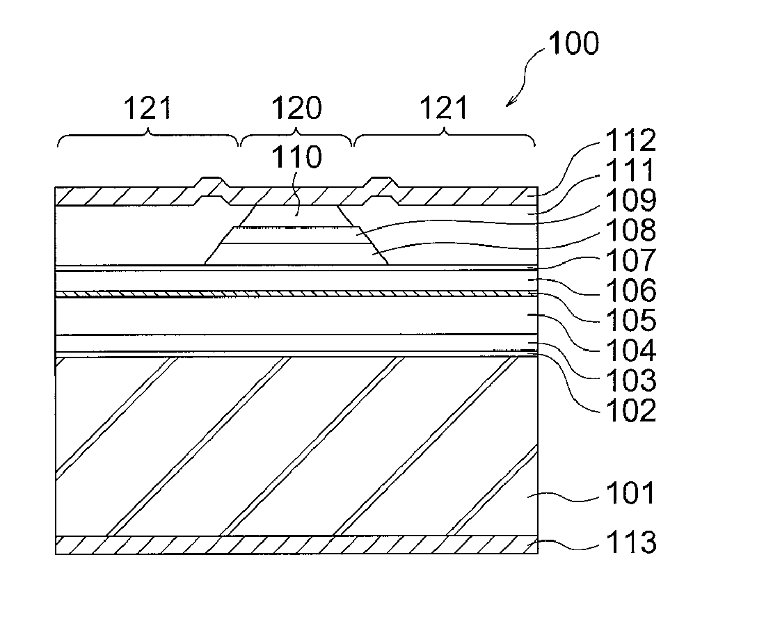
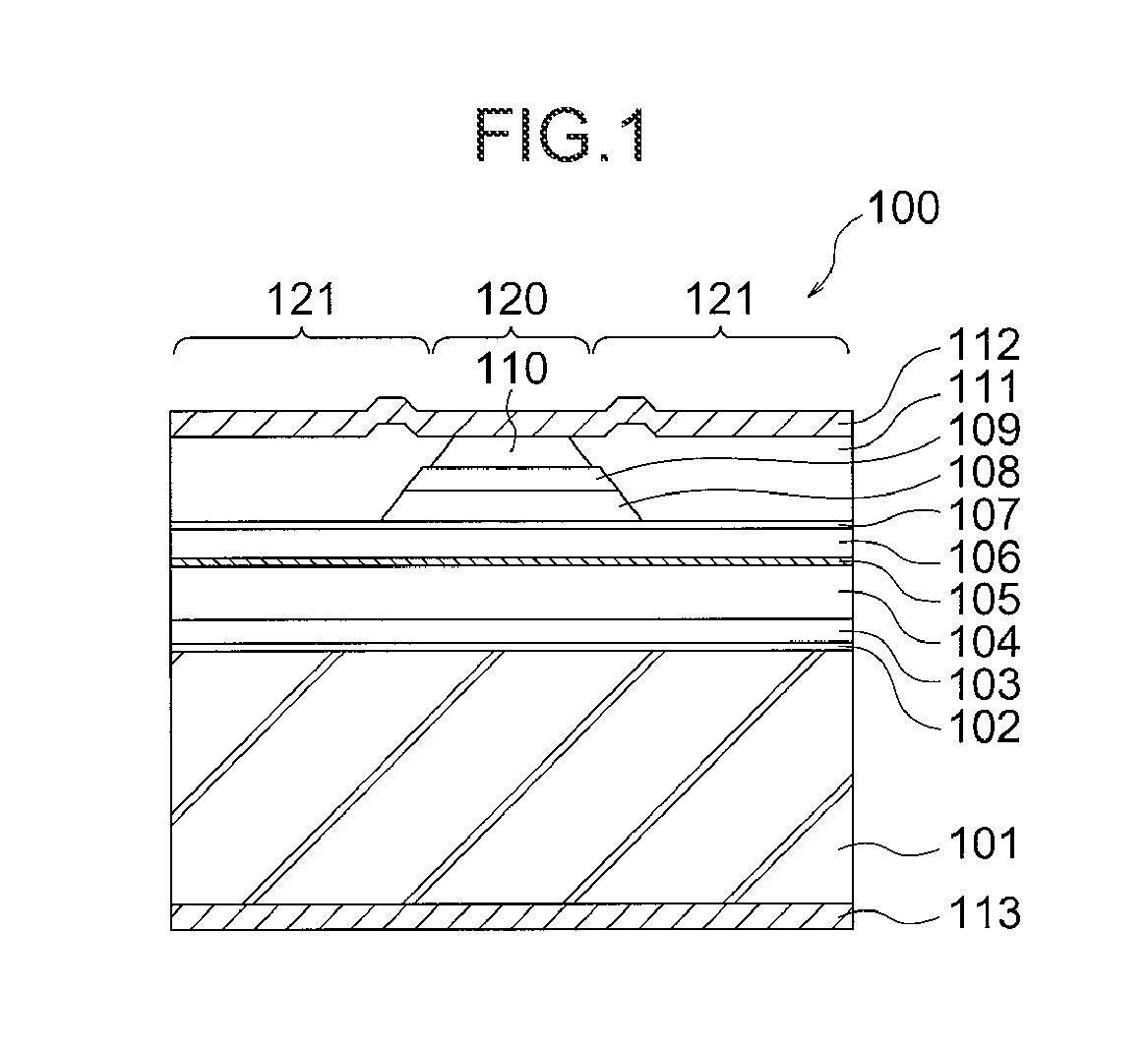
[0081] This example of embodiment relates to an example of semiconductor laser element according to a preferred embodiment of the present invention. FIG. 1 is a cross-sectional view showing a configuration of a semiconductor laser element according to such embodiment.

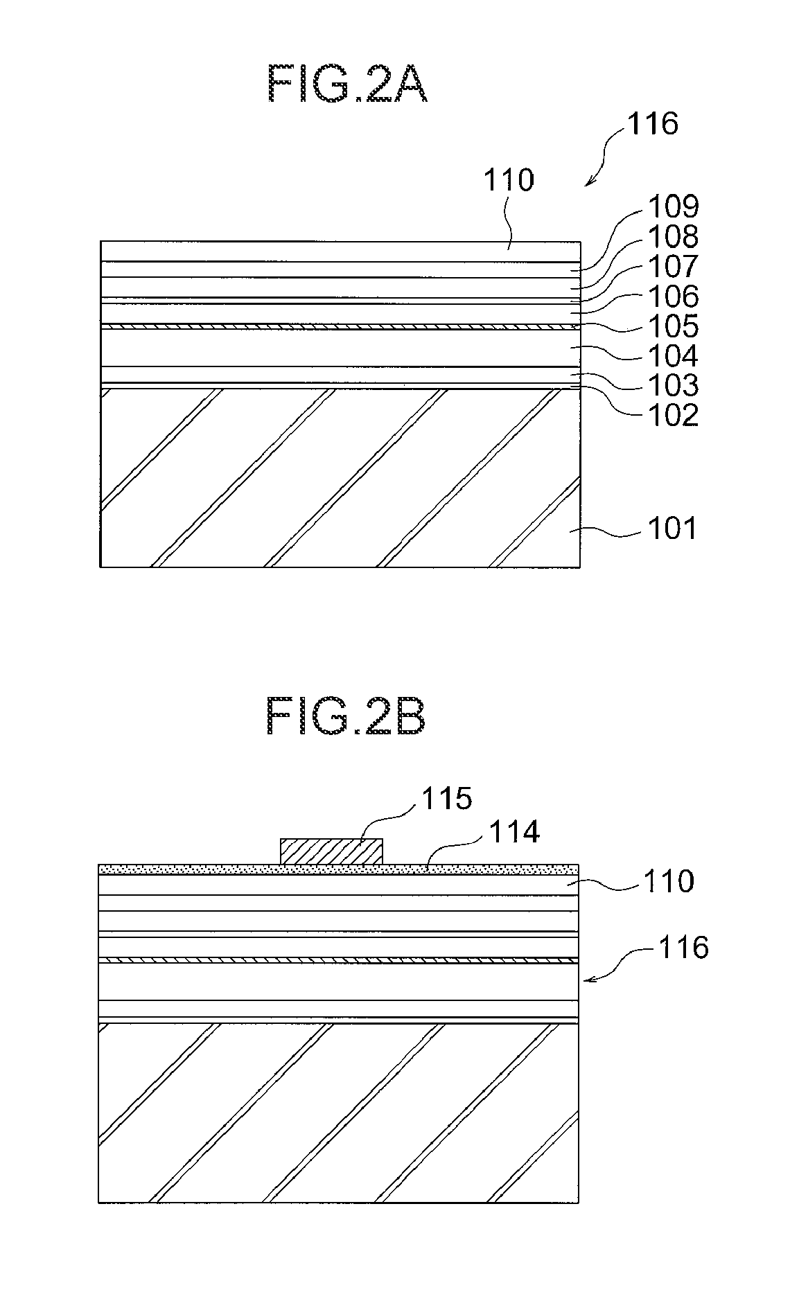
[0082] A semiconductor laser element 100 of this embodiment comprises a stacked structure formed on an n-GaAs substrate 101, where the stacked structure compris...


PUM


Abstract

A semiconductor laser element having an advantageous vertical light confinement efficiency, a low threshold current and a low element resistance is provided. The semiconductor laser element has a substrate and a stacked structure formed thereon, where the stacked structure comprises a buffer layer, an n-Al0.6Ga0.4As cladding layer, an n-Al0.47Ga0.53As cladding layer, an active layer, a p-Al0.47Ga0.53As first cladding layer, an Al0.55Ga0.45As etching stop layer, a p-Al0.47Ga0.53As second cladding layer, a p-Al0.6Ga0.4As third cladding layer, and a p-GaAs contact layer. The second and third cladding layers, and the contact layer are formed as a stripe-patterned ridge, and serve as a current injection regions. Both lateral portions of the ridge are filled with an n-type current blocking layer and serve as non-current-injection regions. Because the cladding layers on the active-layer-section side have a refractive index larger than that of the cladding layers disposed outward thereof, light leaked from the active layer section can efficiently be confined within the cladding layers on the active-layer-section side.

Description

RELATED APPLICATION DATA [0001] This application is a continuation of U.S. patent application Ser. No. 11 / 456,621, filed Aug. 18, 2006, which is a divisional of U.S. patent application Ser. No. 10 / 762,696, filed Jan. 22, 2004, the entirety of both of which are incorporated herein by reference to the extent permitted by law. The present invention claims priority to Japanese patent application No. 2003-014451 filed in the Japanese Patent Office on Jan. 23, 2003, the entirety of which also is incorporated by reference herein to the extent permitted by law.BACKGROUND OF THE INVENTION [0002] 1. Field of the Invention [0003] The present invention relates to a semiconductor laser element and a method of fabricating the same, and more particularly to a AlGaAs-based ridge-stripe semiconductor laser element withlow operational voltage and low element resistance, and a method of fabricating the element. [0004] 2. Description of the Related Art [0005] In recent years, AlGaAs-based infrared wave...

Claims


Application Information

Patent Timeline
Patent Type & Authority Applications(United States)
IPC IPC(8): H01S5/00
CPCB82Y20/00H01S5/209H01S5/2231H01S5/3215H01S5/3432
Inventor SATO, YOSHIFUMI
Owner SATO YOSHIFUMI
Why Eureka
Try Eureka