Plasma etching method and computer-readable storage medium

a technology of etching method and etching method, which is applied in the direction of basic electric elements, semiconductor/solid-state device manufacturing, electric devices, etc., can solve the problems of difficult to obtain a sufficient selectivity with respect to low-k films, and achieve sufficient etching selectivity, prevent undercutting, and high selectivity

Inactive Publication Date: 2007-09-20
TOKYO ELECTRON LTD
View PDF7 Cites 3 Cited by
  • Summary
  • Abstract
  • Description
  • Claims
  • Application Information

AI Technical Summary

Benefits of technology

[0012]In accordance with the present invention, a plasma etching is performed on an etching stop film after plasma-etching a low-k film in a structure where a wiring layer, the etching stop film made of an SiC-based material, the low-k film and an etching mask are formed in that order on a substrate. To plasma-etch the etching stop film, a processing gas containing an NF3 is introduced into a processing chamber while supplying a high frequency power for plasma generation to a first or a second electrode to generate a plasma. Moreover, by applying a DC voltage to any one of the electrodes, deposits are formed on an etching sidewall to thereby protect the sidewall and, further, electrons generated during the plasma formation are accelerated in a vertical direction in a processing space due to the DC voltage. Therefore, the etching can be carried out more anisotropically, which prevents a formation of an undercut. Furthermore, since the NF3 gas having a substantially high selectivity with respect to the low-k film is used as an etching gas, a sufficient etching selectivity can be obtained even when an etching rate of the etching stop film deteriorates due to the deposits.

Problems solved by technology

However, when the etching stop film is etched by using a conventional CF-based etching gas, it is difficult to obtain a sufficient selectivity with respect to the low-k film.

Method used


Image

  • Plasma etching method and computer-readable storage medium
  • Plasma etching method and computer-readable storage medium
  • Plasma etching method and computer-readable storage medium

Examples


Embodiment Construction

[0030]Hereinafter, embodiments of the present invention will be described in detail with reference to the accompanying drawings.

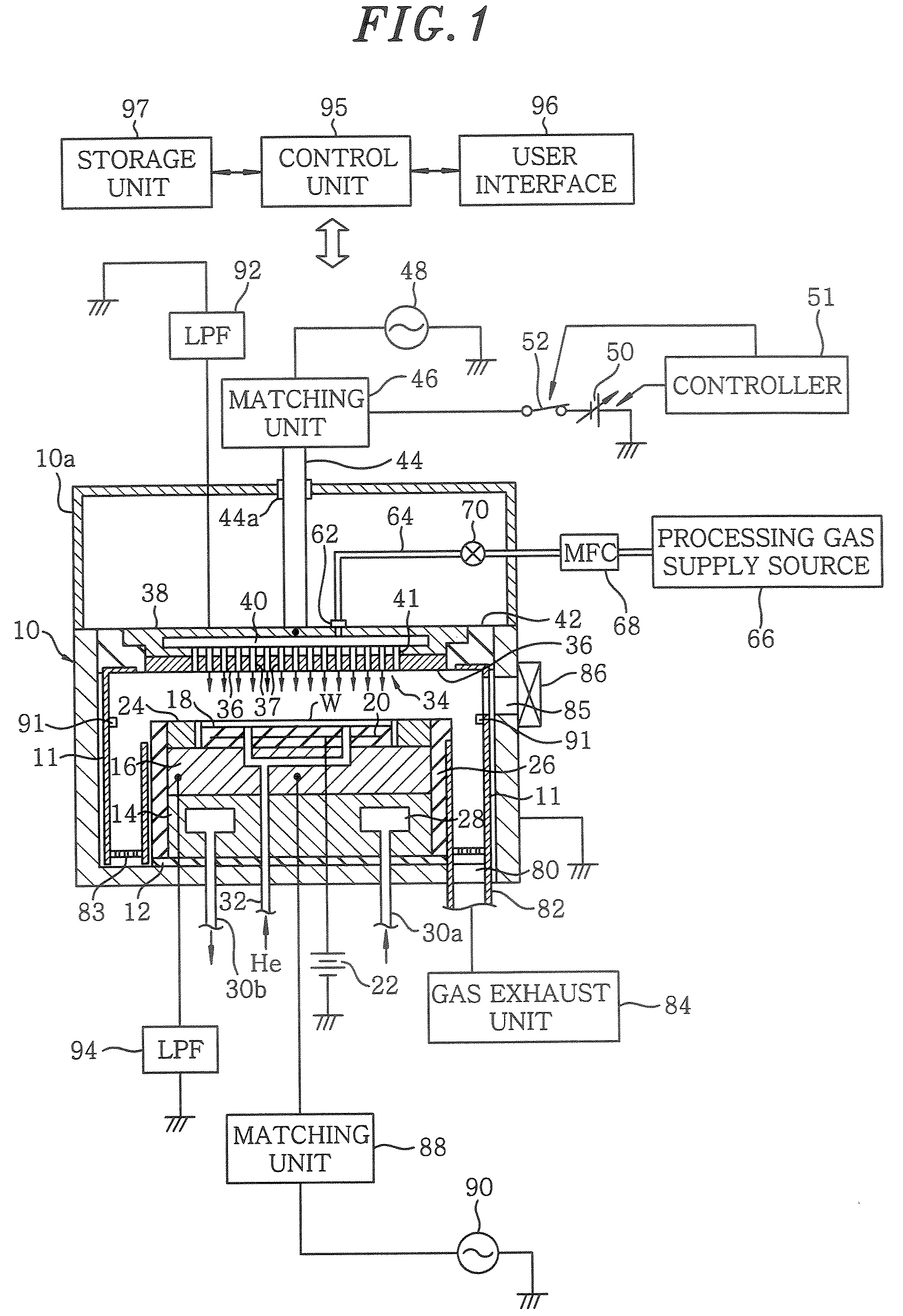
[0031]FIG. 1 is a schematic cross sectional view of an example of a plasma etching apparatus utilized in implementing the present invention.

[0032]This plasma etching apparatus is a capacitance-coupled parallel plate type plasma etching apparatus and includes a substantially cylindrical chamber (processing chamber) 10 made of, e.g. surface-anodized aluminum. The chamber 10 is a frame-grounded.

[0033]On a bottom portion of the chamber 10, there is arranged a cylindrical susceptor support 14 through an insulating plate 12 made of ceramics or other materials. A susceptor 16 made of, e.g., aluminum, is provided on the susceptor support 14, wherein the susceptor 16 is adapted to serve also as a lower electrode. A semiconductor wafer W serving as an object substrate is mounted on the susceptor (lower electrode) 16.

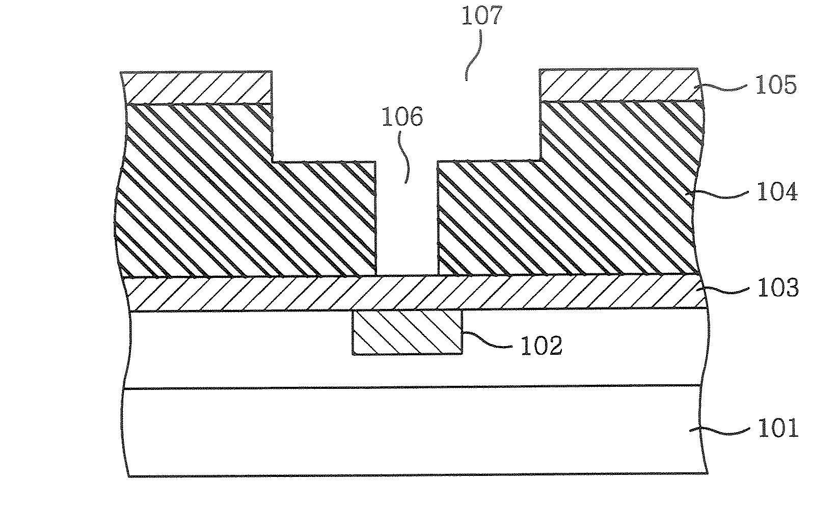
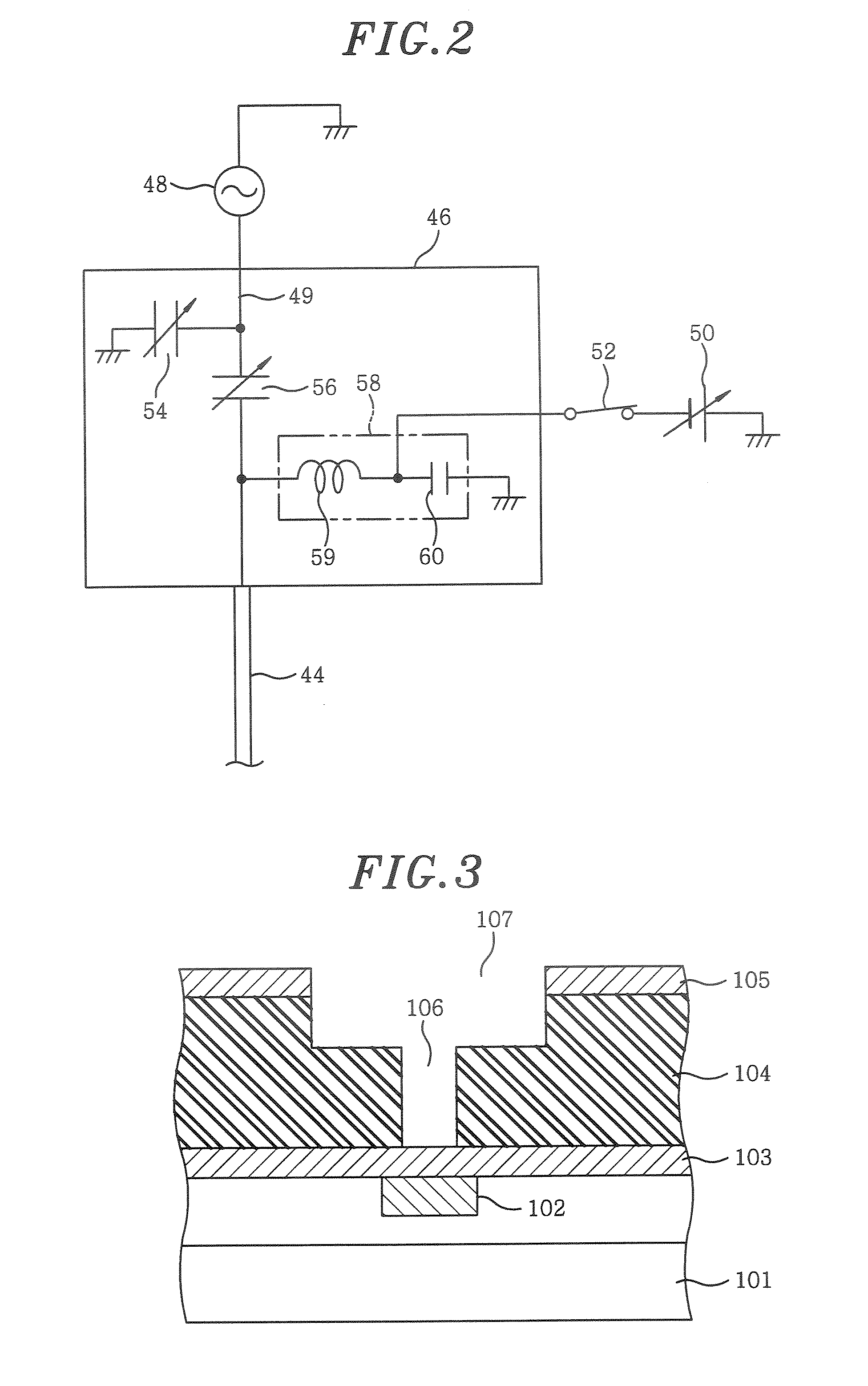
[0034]On a top surface of the susceptor 16, there i...


PUM


Abstract

In a plasma etching method for plasma-etching an etching stop film after plasma-etching a low-k film in a structure in which a wiring layer, the etching stop film made of an SiC-based material, the low-k film and an etching mask are formed in that order on a substrate, the method includes the step of arranging the structure having the plasma-etched low-k film in a processing chamber in which a first and a second electrode are provided to face each other at vertically separated locations. The plasma etching method further includes the steps of introducing a processing gas containing NF3 into the processing chamber; generating a plasma by applying a high frequency power to one of the first and the second electrode; and applying a DC voltage to said one of the electrodes.

Description

FIELD OF THE INVENTION[0001]The present invention relates to a plasma etching method and a computer-readable storage medium storing the plasma etching method, wherein the plasma etching method serves to plasma-etch an etching stop film after plasma-etching a low-k film in a structure where a wiring layer, the etching stop film made of an SiC-based material, the low-k film and an etching mask are formed in that order on a substrate.BACKGROUND OF THE INVENTION[0002]A miniaturization of semiconductor devices reduces a distance between wirings and, therefore, an inter-wiring capacitance increases. Accordingly, a signal propagation speed is reduced, which in turn reduces an operating speed. To that end, there are being developed an interlayer insulating film made of an insulating material having a low dielectric constant (low-k material), i.e., a low-k film, and a multilayer interconnection using same. Meanwhile, copper having low resistance and high electromigration tolerance has been n...

Claims


Application Information

Patent Timeline
Patent Type & Authority Applications(United States)
IPC IPC(8): H01L21/467
CPCH01L21/31116H01L21/31138H01L21/76829H01L21/7681H01L21/76804
Inventor YOSHIDA, RYOICHI
Owner TOKYO ELECTRON LTD
Why Eureka
Try Eureka