
Package device with electromagnetic interference shield

Active Publication Date: 2007-05-03
CYNTEC
View PDF11 Cites 17 Cited by
  • Summary
  • Abstract
  • Description
  • Claims
  • Application Information

AI Technical Summary

Benefits of technology

[0009] In accordance with the above background prior art, in order to solve the electromagnetic / radio frequency interference for the package device, the present invention provides a package device with electromagnetic interference shield, whereby the power density of the package device system can be increased.
[0010] It is another object of this invention to provide a shield structure that located between the substrate and insulating layer. The electromagnetic / radio frequency can be discharged to the outside of the package device from the substrate through the metal plate to the grounded. Thus, the other system would not be affected by the electromagnetic / radio frequency interference in the package device. Also, the immunity against the electromagnetic / radio frequency interference can be increased.

Problems solved by technology

Because of the electromagnetic interference is generated from the electronic equipment and the restraint is generated from the environment of the electronic equipment, the electromagnetic compatibility for the electronic equipment is an important issue to consider.
In general, the electromagnetic / radio frequency interference would be caused by the package device is that the interaction between the every electronic devices located on the package device.
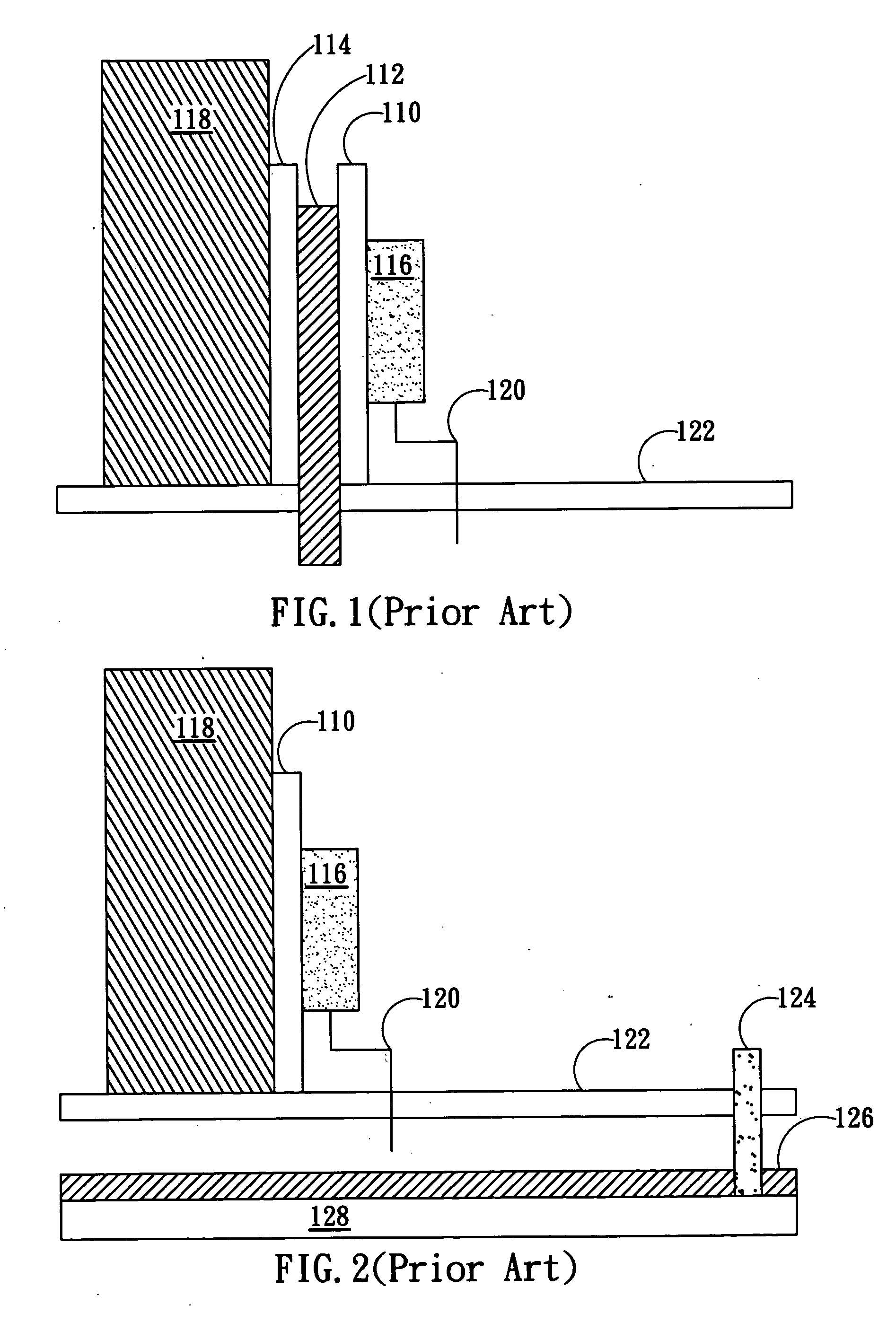
However, the heat dissipating capability is not good for the insulating layer 114.
According to the above discussion would be obtained the heat dissipating path for the package device, but the fabricating of the package device is still difficult and the cost would be increased.

Method used


Image

  • Package device with electromagnetic interference shield
  • Package device with electromagnetic interference shield
  • Package device with electromagnetic interference shield

Examples


Embodiment Construction

[0023] Some sample embodiments of the invention will now be described in greater detail. Nevertheless, it should be recognized that the present invention can be practiced in a wide range of other embodiments besides those explicitly described, and the scope of the present invention is expressly not limited except as specified in the accompanying claims.

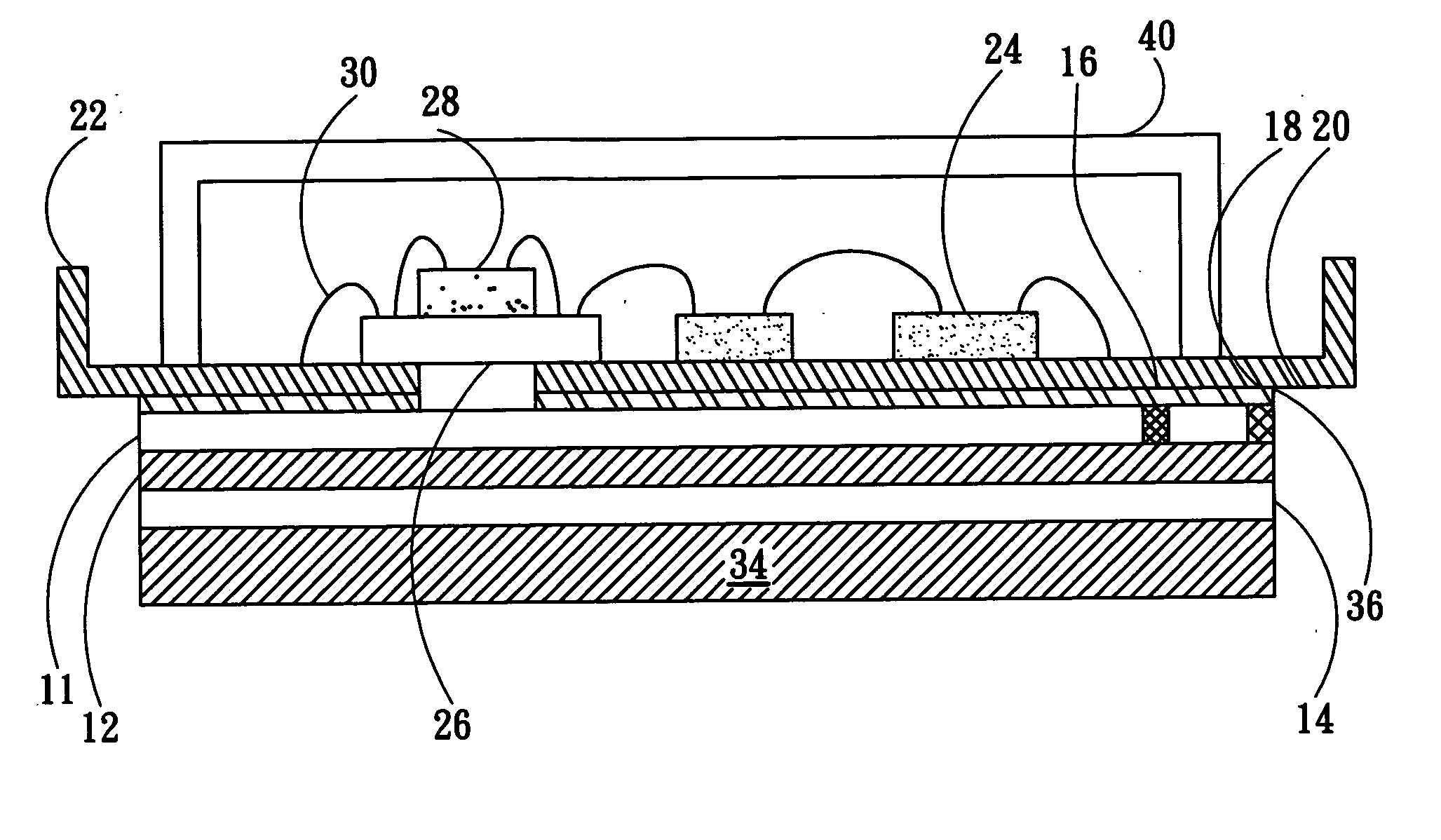
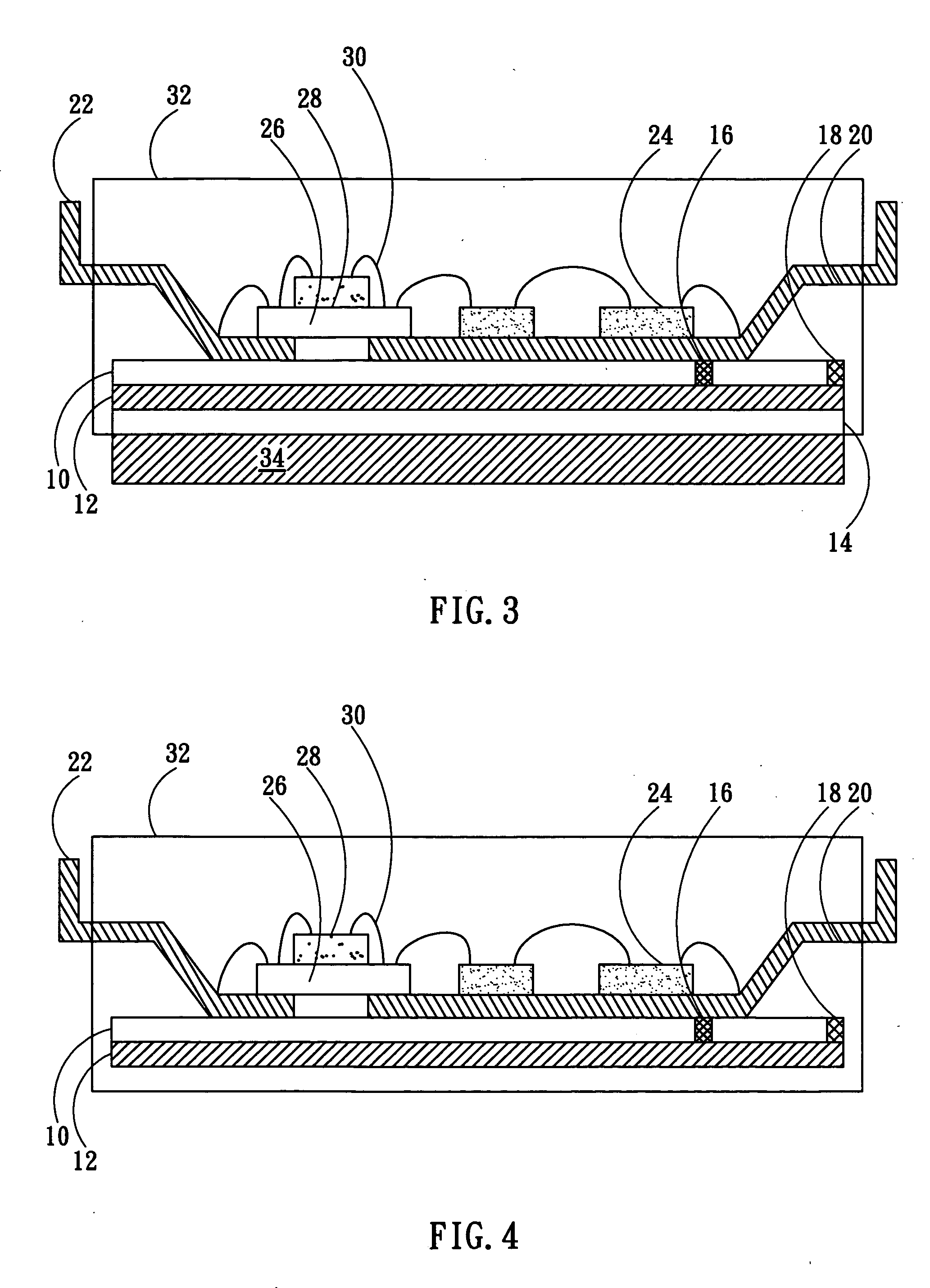
[0024]FIG. 3 shows the preferred embodiment of the present invention for the package device with electromagnetic interference shield. The package device with an electromagnetic interference shield includes a first substrate 10 without wirings thereon / therein, a shielding structure 12, a plurality of lead-frames 20, a plurality of first electronic devices 24, a second substrate 26, a plurality of second electronic devices 28, and a plurality of conductive wires 30.

[0025] The shielding structure 12 located under the bottom surface of the first substrate 10 without wirings, the insulating layer 14 located under the shielding structure ...


PUM


Abstract

The present invention provides a package device for reducing the electromagnetic / radio frequency interference, which includes a first substrate with a shielding structure on the under surface of the first substrate, and an insulating layer on the shielding structure. The first substrate includes a through hole that is filled with the conductor therein. A plurality of lead-frames located on the bottom surface of the first substrate. A second substrate located above between the two lead-frames. Then, the molding compound encapsulated to cover the above structures to form a package device. Therefore, the shielding path of the package device is constructed of the plurality of lead-frames, the conductor within the first substrate, the shielding structure, and the grounded to discharge the electromagnetic / radio frequency out of the package device, thus, the electromagnetic / radio frequency interference for the package device can be reduced.

Description

BACKGROUND OF THE INVENTION [0001] 1. Field of the Invention [0002] The present invention generally relates to a package device, particularly to indicate to a package device with electromagnetic interference shield. [0003] 2. Description of the Prior Art [0004] In recently, the electrical technology is developed rapidly, and the electronic equipment is used for widely application. Because of the electromagnetic interference is generated from the electronic equipment and the restraint is generated from the environment of the electronic equipment, the electromagnetic compatibility for the electronic equipment is an important issue to consider. The objective of the shielding structure is that preventing the performance of other electronic devices is to be reduced, or the damage to the inside electronic device. [0005] In general, the electromagnetic / radio frequency interference would be caused by the package device is that the interaction between the every electronic devices located on ...

Claims


Application Information

Patent Timeline
IPC IPC(8): H01L23/12H01L23/52
CPCH01L23/3107H01L23/36H01L23/4334H01L23/495H01L23/552H01L23/66H01L24/49H01L25/072H01L2224/48091H01L2224/48137H01L2224/48145H01L2224/48247H01L2224/49H01L2224/73265H01L2924/01004H01L2924/01082H01L2924/16152H01L2924/19107H01L2924/30107H01L2924/3025H01L2924/00014H01L24/48H01L2924/01006H01L2924/01033H01L2924/00H01L2924/181H01L2224/45099H01L2924/00012
Inventor WEN, CHAU CHUNCHEN, DA-JUNGLIN, CHUN-LIANGDAY, CHIH-CHAN
Owner CYNTEC
Learn More