Semiconductor integrated circuit device

a technology of integrated circuit device and semiconductor, applied in the direction of power supply for data processing, instruments, computing, etc., can solve the problems of inability to achieve effective power consumption reduction and control the state, and achieve the effect of low power consumption operation and efficient power supply control

Active Publication Date: 2007-05-03
RENESAS ELECTRONICS CORP
View PDF12 Cites 39 Cited by
  • Summary
  • Abstract
  • Description
  • Claims
  • Application Information

AI Technical Summary

Benefits of technology

[0012] Accordingly, an object of the present invention is to provide a technology capable of performing an efficient power supply

Problems solved by technology

However, the inventors of the present invention have found the following problems in the technology for low power consumption described above.
However, in the above-described R-standby mode and the U-standby mode, it is difficult to co

Method used


Image

  • Semiconductor integrated circuit device
  • Semiconductor integrated circuit device
  • Semiconductor integrated circuit device

Examples


Embodiment Construction

[0035] Hereinafter, embodiments of the present invention will be described in detail with reference to the accompanying drawings. Note that components having the same function are denoted by the same reference symbols throughout the drawings for describing the embodiment, and the repetitive description thereof will be omitted.

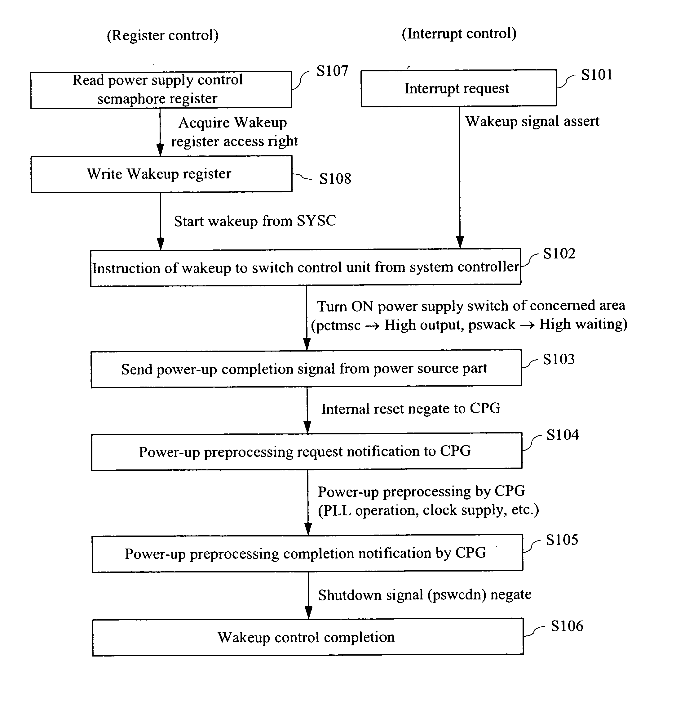
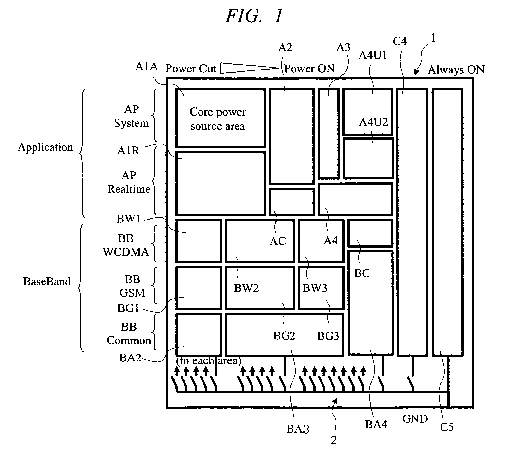
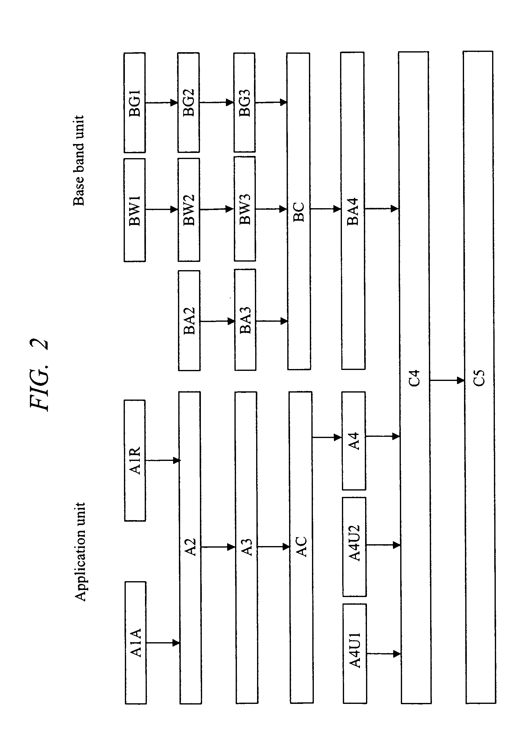
[0036]FIG. 1 is an explanatory diagram showing power source areas in a semiconductor integrated circuit device according to an embodiment of the present invention. FIG. 2 is an explanatory diagram showing the hierarchical relations of core power source areas in the semiconductor integrated circuit device in FIG. 1. FIG. 3 is an explanatory diagram showing the structure of a power supply control unit provided in the semiconductor integrated circuit device in FIG. 1. FIG. 4 is an explanatory diagram showing a WUC which generates a wakeup signal to be inputted to a complementary logic unit provided in the semiconductor integrated circuit device in FIG. 1. FIG. 5 ...


PUM


Abstract

The power supply is effectively controlled in a semiconductor integrated circuit device having a multi domain structure so as to reduce the power consumption. When an interrupt signal is inputted, the system controller makes an instruction of wakeup to the corresponding switch control unit. At this moment, the system controller controls power supply so as to be supplied sequentially from the core power source area belonging to the lower hierarchical level dependent on the core power source area to which power is supplied. The system controller outputs the power supply switch-on request signal to the switch control unit. The switch control unit turns ON the power supply switch and sends the power-on completion signal back to the system controller. Similarly, the system controller supplies power sequentially to core power source areas in the dependency relation one after another from the lower hierarchy to the upper hierarchy.

Description

CROSS-REFERENCE TO RELATED APPLICATION [0001] The present application claims priority from Japanese Patent Application No. JP 2005-314137 filed on Oct. 28, 2005, the content of which is hereby incorporated by reference into this application. TECHNICAL FIELD OF THE INVENTION [0002] The present invention relates to a technology for reducing the power consumption in a semiconductor integrated circuit device. More specifically, it relates to a technology effectively applied to the reduction of power consumption in a semiconductor integrated circuit device having a multi domain structure. BACKGROUND OF THE INVENTION [0003] In recent years, a cellular phone has spread widely as one of mobile communication devices, and the multifunctionality has been required for the mobile devices. For example, in a semiconductor integrated circuit device used in the cellular phone, the demand for low power consumption has been extremely strong. [0004] As the technology for low power consumption in this k...

Claims


Application Information

Patent Timeline
IPC IPC(8): G06F1/00
CPCG06F1/3203
Inventor TSUKIMORI, AKIFUMIIRITA, TAKAHIROKATO, HISASHI
Owner RENESAS ELECTRONICS CORP
Why Eureka
Try Eureka