Oxide semiconductor transistor and manufacturing method thereof

a manufacturing method and semiconductor technology, applied in the field of semiconductor transistors, can solve the problems of low leakage current of the transistor including the oxide semiconductor layer, gate voltage (vg) and drain voltage (vd) are also too high, and achieve the effect of reducing the sub-threshold swing (ss) and increasing the on-curren

Active Publication Date: 2017-08-01
UNITED MICROELECTRONICS CORP
View PDF4 Cites 39 Cited by
  • Summary
  • Abstract
  • Description
  • Claims
  • Application Information

AI Technical Summary

Benefits of technology

[0005]An oxide semiconductor transistor and a manufacturing method thereof are provided by the present invention. A ferroelectric material layer is disposed between a metal gate and an internal electrode for forming a negative capacitance effect. The on-current of the oxide semiconductor transistor may be enhanced, and the oxide semiconductor transistor may be applied in low power operation accordingly.
[0008]In the oxide semiconductor transistor of the present invention, the ferroelectric material layer and the internal electrode disposed between the metal gate and the gate insulation layer may be used to form a negative capacitance effect, and the negative capacitance effect may be used to amplify the gate voltage. The purposes of increasing the on-current and lowering the sub-threshold swing (SS) may be achieved accordingly. In addition, the gate insulation layer may become thinner without influencing the low leakage current performance because of the ferroelectric material layer, the oxide semiconductor transistor may be used in low power operations, and the application field of the oxide semiconductor transistor may be expanded accordingly.

Problems solved by technology

However, although the leakage current of the transistor including the oxide semiconductor layer is relatively low, the application field of the present oxide semiconductor transistor is still limited because the threshold voltage (Vt) of the oxide semiconductor transistor is still too high and the on-current (Ion) of the oxide semiconductor transistor is not high enough for some application such as low power devices.
The gate voltage (Vg) and the drain voltage (Vd) are also too high because of the relatively higher threshold voltage of the oxide semiconductor transistor, and the oxide semiconductor transistor cannot be applied in the low power devices accordingly.

Method used


Image

  • Oxide semiconductor transistor and manufacturing method thereof
  • Oxide semiconductor transistor and manufacturing method thereof
  • Oxide semiconductor transistor and manufacturing method thereof

Examples


first embodiment

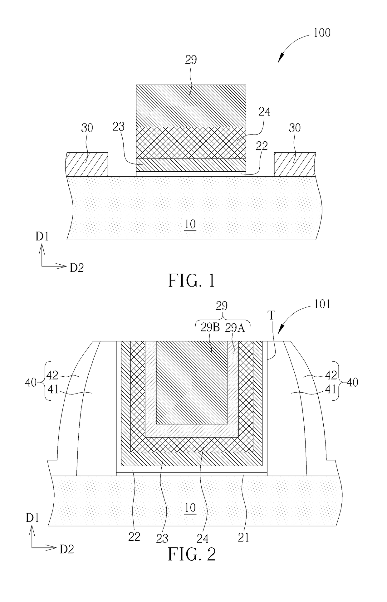
[0023]Please refer to FIG. 1. FIG. 1 is a schematic drawing illustrating an oxide semiconductor transistor according to the present invention. As shown in FIG. 1, an oxide semiconductor transistor 100 is provided in this embodiment. The oxide semiconductor transistor 100 includes an oxide semiconductor channel layer 10, a metal gate 29, a gate insulation layer 22, an internal electrode 23, and a ferroelectric material layer 24. The metal gate 29 is disposed on the oxide semiconductor channel layer 10. The gate insulation layer 22 is disposed between the metal gate 29 and the oxide semiconductor channel layer 10. The internal electrode 23 is disposed between the gate insulation layer 22 and the metal gate 29. The ferroelectric material layer 24 is disposed between the internal electrode 23 and the metal gate 29. In other words, the gate insulation layer 22, the internal electrode 23, the ferroelectric material layer 24, and the metal gate 29 are stacked sequentially on the oxide semi...

second embodiment

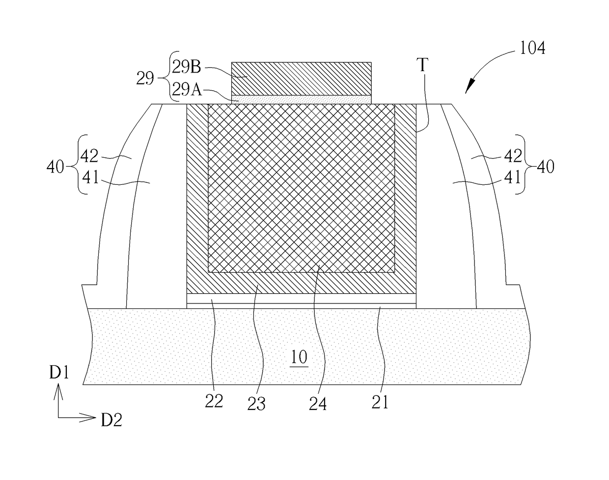
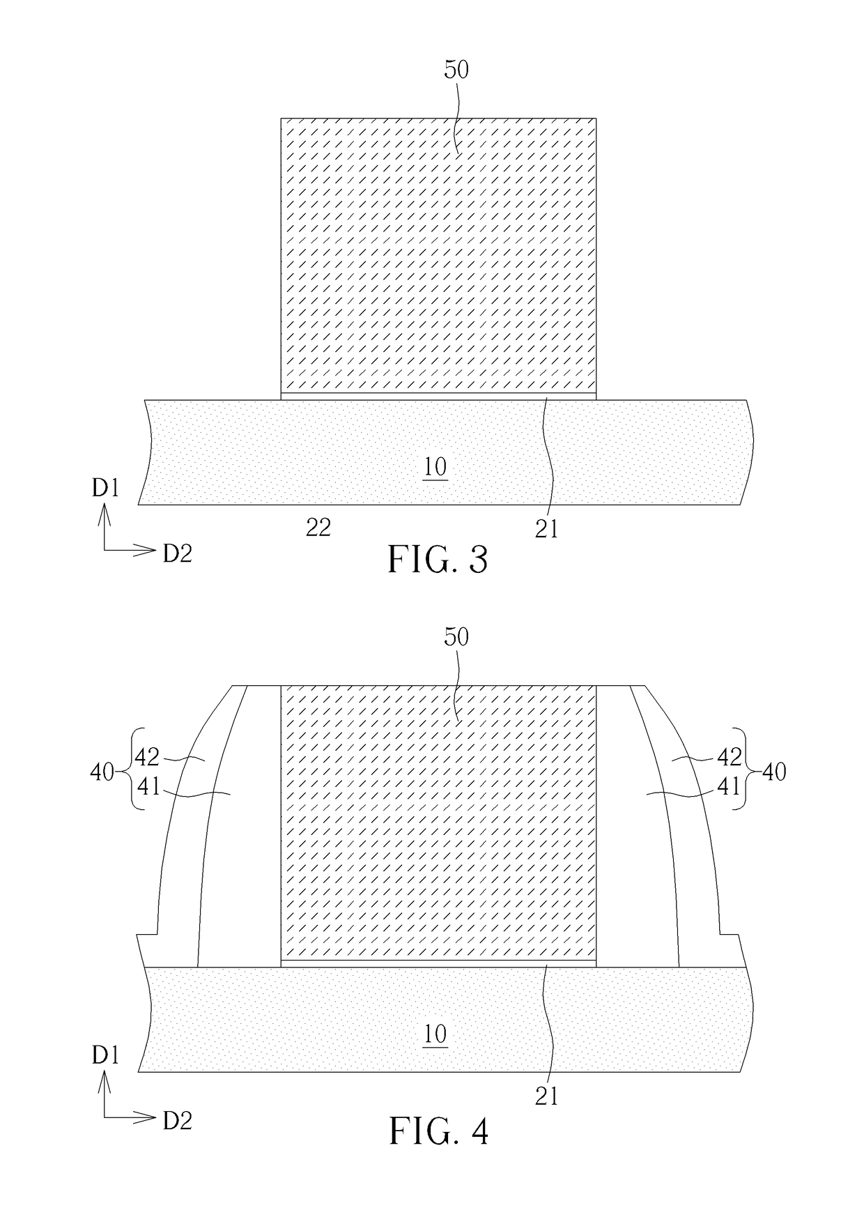
[0033]Please refer to FIGS. 2-5. FIGS. 3-5 are schematic drawings illustrating a manufacturing method of the oxide semiconductor transistor 101 according to the present invention. The manufacturing method of the oxide semiconductor transistor 101 in this embodiment may include the following steps. As shown in FIG. 3, the interface layer 21 and a dummy gate 50 are formed on the oxide semiconductor channel layer 10. The dummy gate 50 and the interface layer 21 may be formed by patterning material layers on the oxide semiconductor channel layer 10 simultaneously, such as by etching processes with the same patterned mask, but not limited thereto. As shown in FIG. 4, the spacer 40 is then formed on the oxide semiconductor channel layer 10, and the spacer 40 is formed on sidewalls of the dummy gate 50 and the interface layer 21. In other words, the dummy gate 50 is formed before the step of forming the spacer 40. The first spacer 41 may be formed by a process of forming a conformal materi...


PUM


Abstract

An oxide semiconductor transistor includes an oxide semiconductor channel layer, a metal gate, a gate insulation layer, an internal electrode, and a ferroelectric material layer. The metal gate is disposed on the oxide semiconductor channel layer. The gate insulation layer is disposed between the metal gate and the oxide semiconductor channel layer. The internal electrode is disposed between the gate insulation layer and the metal gate. The ferroelectric material layer is disposed between the internal electrode and the metal gate. The ferroelectric material layer in the oxide semiconductor transistor of the present invention is used to enhance the electrical characteristics of the oxide semiconductor transistor.

Description

BACKGROUND OF THE INVENTION[0001]1. Field of the Invention[0002]The present invention relates to a transistor and a manufacturing method thereof, and more particularly, to an oxide semiconductor transistor including a ferroelectric material layer and a method of forming the same.[0003]2. Description of the Prior Art[0004]Oxide semiconductor materials, such as indium gallium zinc oxide (IGZO), have been applied in thin film transistors (TFTs) of display devices and field effect transistors (FETs) used in integrated circuits because of properties such as high mobility and low leakage current. However, although the leakage current of the transistor including the oxide semiconductor layer is relatively low, the application field of the present oxide semiconductor transistor is still limited because the threshold voltage (Vt) of the oxide semiconductor transistor is still too high and the on-current (Ion) of the oxide semiconductor transistor is not high enough for some application such ...

Claims


Application Information

Patent Timeline
Patent Type & Authority Patents(United States)
IPC IPC(8): H01L21/28H01L29/06H01L29/423H01L29/66H01L27/11585H01L29/786H01L29/51
CPCH01L29/7869H01L29/516H01L29/0649H01L29/4236H01L29/66969H01L21/28291H01L27/11585H01L29/6684H01L29/4908H01L29/40111H10B51/00
Inventor XING, SUWANG, HSUEH-WENKO, CHIEN-YUTUNG, YU-CHENGWANG, JEN-YUHUANG, CHENG-TUNGLIN, YU-MING
Owner UNITED MICROELECTRONICS CORP
Why Eureka
Try Eureka