Logic switching device and method of manufacturing the same

a switching device and logic technology, applied in the direction of manufacturing tools, basic electric elements, soldering apparatus, etc., can solve the problems of increasing power density, difficult to lower the operating voltage to about 0.8 v or less, and limited improvement of operating characteristics and scaling down of existing silicon-based transistors, etc., to achieve negative capacitance effect, improve operating characteristics, and increase control efficiency

Active Publication Date: 2020-07-07
SAMSUNG ELECTRONICS CO LTD
View PDF16 Cites 0 Cited by
  • Summary
  • Abstract
  • Description
  • Claims
  • Application Information

AI Technical Summary

Benefits of technology

[0007]Provided is a logic switching device using a negative capacitance effect. Provided is a logic switching device using a ferroelectric material and an anti-ferroelectric material. Provided is a logic switching device with improved operating characteristics such as subthreshold swing (SS) and / or increased control efficiency and / or advantageous for scaling down. Provided is a method of manufacturing the logic switching device.

Problems solved by technology

Improving the operating characteristics and scaling down of existing silicon-based transistors are limited.
As the size of the transistors decreases, a power density increases due to factors that make it difficult to lower the operating voltage to about 0.8 V or less.
Therefore, scaling down of devices is limited.

Method used


Image

  • Logic switching device and method of manufacturing the same
  • Logic switching device and method of manufacturing the same
  • Logic switching device and method of manufacturing the same

Examples


Embodiment Construction

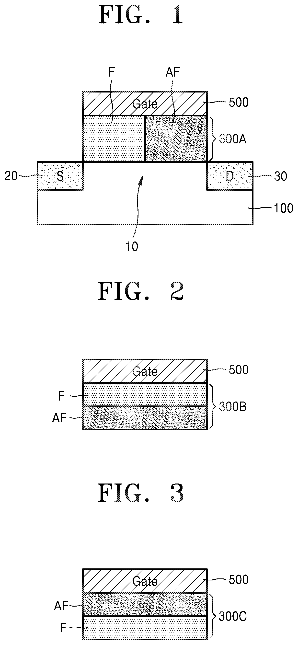
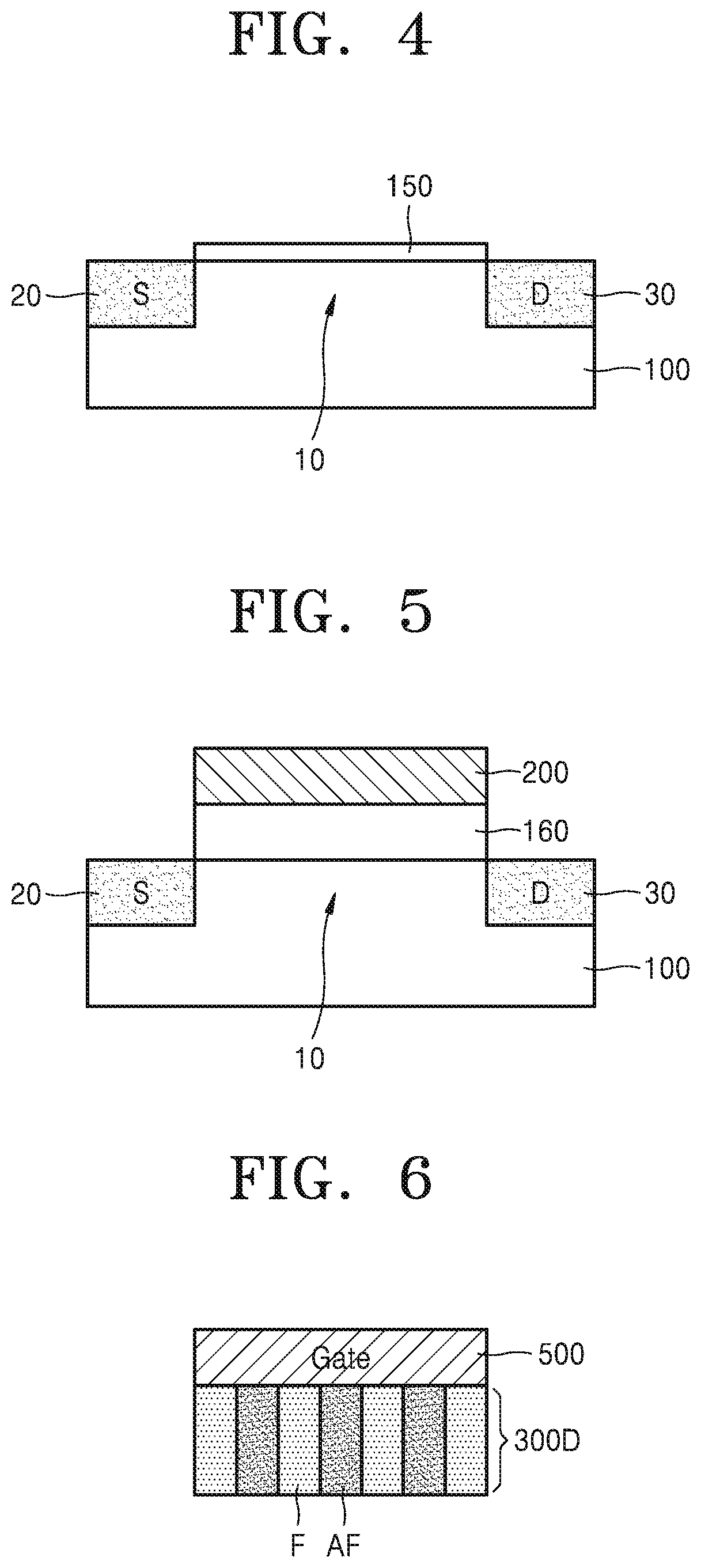
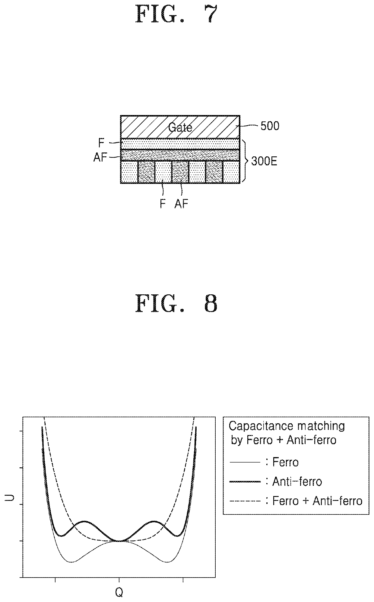
[0056]Various example embodiments will now be described more fully with reference to the accompanying drawings in which example embodiments are shown.

[0057]It will be understood that when an element is referred to as being “connected” or “coupled” to another element, it can be directly connected or coupled to the other element or intervening elements may be present. In contrast, when an element is referred to as being “directly connected” or “directly coupled” to another element, there are no intervening elements present. As used herein the term “and / or” includes any and all combinations of one or more of the associated listed items.

[0058]It will be understood that, although the terms “first”, “second”, etc. may be used herein to describe various elements, components, regions, layers and / or sections, these elements, components, regions, layers and / or sections should not be limited by these terms. These terms are only used to distinguish one element, component, region, layer or secti...


PUM

PropertyMeasurementUnit
temperatureaaaaaaaaaa
thicknessaaaaaaaaaa
thicknessaaaaaaaaaa

Abstract

Provided are a logic switching device and a method of manufacturing the same. The logic switching device may include a domain switching layer adjacent to a gate electrode. The domain switching layer may include a ferroelectric material region and an anti-ferroelectric material region. The domain switching layer may be a non-memory element. The logic switching device may include a channel, a source and a drain both connected to the channel, the gate electrode arranged to face the channel, and the domain switching layer provided between the channel and the gate electrode.

Description

CROSS-REFERENCE TO RELATED APPLICATIONS[0001]This application claims the benefit of Korean Patent Application No. 10-2018-0096828, filed on Aug. 20, 2018 and Korean Patent Application No. 10-2019-0008347, filed on Jan. 22, 2019, in the Korean Intellectual Property Office, the disclosures of which are incorporated herein in their entireties by reference.BACKGROUND1. Field[0002]The present disclosure relates to logic switching devices and methods of manufacturing the same.2. Description of the Related Art[0003]Improving the operating characteristics and scaling down of existing silicon-based transistors are limited. For example, when an operating voltage and current characteristics of the existing silicon-based transistors are measured, a subthreshold swing (SS) value is determined according to the following equation. A subthreshold swing (SS) value is known to be a limit of about 60 mV / dec.[0004]SS=kB⁢Tq⁢ln⁡(10)⁢(1+CDCins)[0005]In the above equation, kB is a Boltzmann constant, T is ...

Claims


Application Information

Patent Timeline
Patent Type & Authority Patents(United States)
IPC IPC(8): B23K3/08B23K3/06H01L23/00
CPCH01L24/26B23K3/08B23K3/0607H01L29/78H01L29/7841H01L29/0603H01L29/0684H01L29/66477H01L29/516H01L29/512H01L29/513H01L29/78391H10B51/30H01L29/6684H10B51/00
Inventor HEO, JINSEONGLEE, YUNSEONGJO, SANGHYUN
Owner SAMSUNG ELECTRONICS CO LTD
Why Eureka
Try Eureka