Semiconductor package with interposer block therein

a technology of interposer block and semiconductor, which is applied in the direction of semiconductor device, semiconductor/solid-state device details, electrical apparatus, etc., can solve the problems of reducing the size of the package, affecting the shape of the package, and not being suitable for a slim and small packag

Inactive Publication Date: 2012-11-15
NEPES CO LTD
View PDF2 Cites 44 Cited by
  • Summary
  • Abstract
  • Description
  • Claims
  • Application Information

AI Technical Summary

Problems solved by technology

However, a high functional semiconductor package needs an additional package substrate to embed semiconductor chips or devices therein, and also requires to have a complicated wiring and metallization structure for connecting devices thereto.
Current used package substrates (such as a Print...

Method used


Image

  • Semiconductor package with interposer block therein
  • Semiconductor package with interposer block therein
  • Semiconductor package with interposer block therein

Examples


Embodiment Construction

[0026]The present invention will now be described more fully hereinafter with reference to the accompanying drawings, in which preferred embodiments of the invention are shown. The present invention relates to a new substrate for a 3-dimensional semiconductor package. The substrate may have various semiconductor devices mounted on one or both surfaces of it and can have a semiconductor device or other electronic device embedded therein, so that a semiconductor package may have a variety of structure and the size of the package can be remarkably reduced.

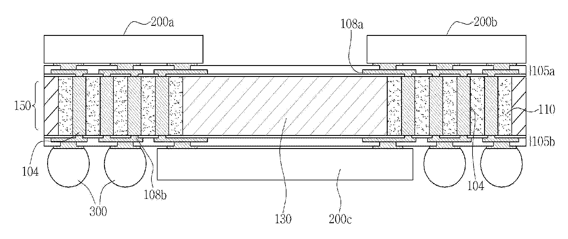
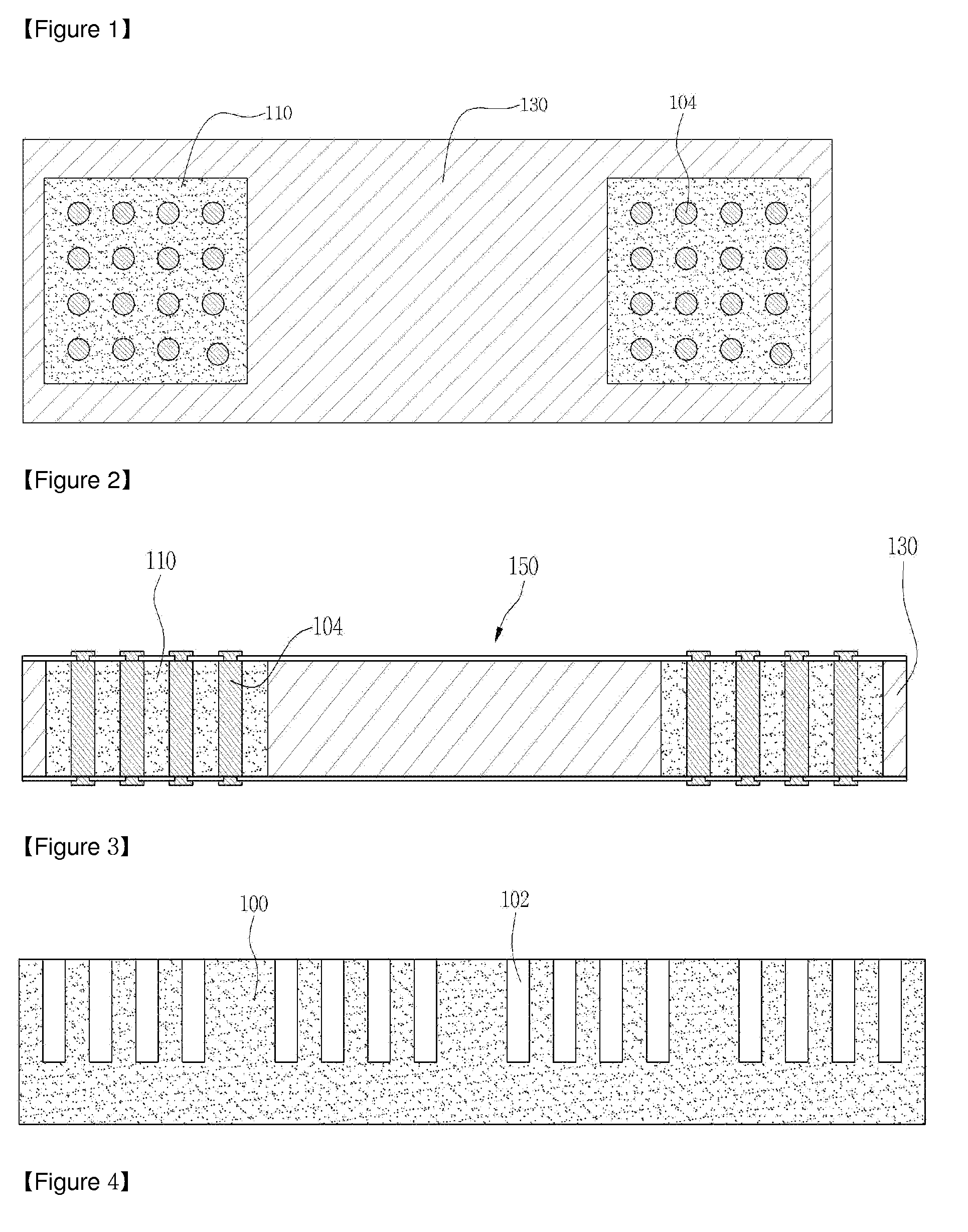
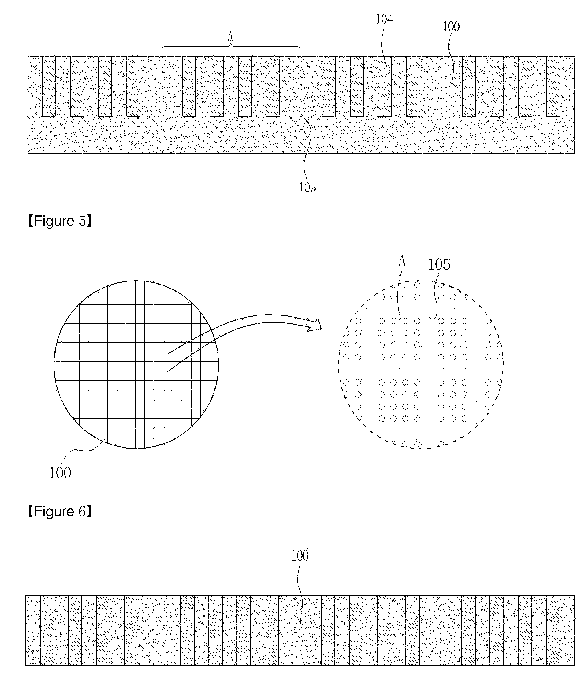
[0027]FIGS. 1 and 2 show a semiconductor package substrate (150) in accordance with the present invention. Interposer blocks (110) are embedded in a mold base (130). The mold base may be formed in a desired geometrical figure, and the interposer block can have a diverse structure needed for a package. The interposer block may include a plurality of sub blocks. In this regard, the sub blocks in the mold base may be arranged apart (or s...


PUM


Abstract

A semiconductor package substrate is provided. The package substrate includes a mold base and an interposer block embedded in the mold base, said interposer block having a plurality of vertical conductive lines therein. A metallization layer is formed on the surface of the interposer block or the mold base, said metallization layer being electrically connected to at least one of the vertical conductive lines. A semiconductor chip may be mounted on or embedded in the mold base.

Description

TECHNICAL FIELD[0001]The present invention relates to a semiconductor package, and more particularly, to a new semiconductor package with an interposer block therein.BACKGROUND ART[0002]A semiconductor component includes a semiconductor substrate containing various semiconductor devices and integrated circuits. Typically, the semiconductor substrate is in the form of a semiconductor die, that has been singulated from a semiconductor wafer. For example, a chip scale semiconductor component includes a semiconductor die provided with support and protective elements, and a signal transmission system. Semiconductor components can also include multiple semiconductor substrates in a stacked or planar array.[0003]It is well known that the consumers of the next generation electronic devices are demanding increased functions and features that are packed in a smaller size, consuming less power, and costing less than the earlier generation. Semiconductor device manufacturers are responding by i...

Claims


Application Information

Patent Timeline
IPC IPC(8): H01L25/07H01L21/50H01L23/48
CPCH01L23/3107H01L25/105H01L2924/0002H01L25/0655H01L25/0657H01L2225/06517H01L2225/1058H01L2225/06572H01L2924/15311H01L25/16H01L2225/1052H01L23/49838H01L21/486H01L23/5384H01L2924/00H01L23/48H01L23/045H01L23/055
Inventor KWON, YONG TAEJUNG, GI JO
Owner NEPES CO LTD
Why Eureka
Try Eureka