Semiconductor device and semiconductor substrate, and method of fabricating the same

a semiconductor and substrate technology, applied in the field of semiconductor devices, can solve the problems of deteriorating the performance of semiconductor transistor elements, reducing the life time and reliability, and reducing the mobility of carriers, so as to improve the operational characteristics, reduce the density of lattice defects, and improve the effect of reliability and performan

Inactive Publication Date: 2004-11-09
XIAMEN SANAN OPTOELECTRONICS CO LTD
View PDF30 Cites 44 Cited by
  • Summary
  • Abstract
  • Description
  • Claims
  • Application Information

AI Technical Summary

Benefits of technology

According to the present invention, a semiconductor layer in a semiconductor layered structure is grown in a certain direction in accordance with the shape of an upper surface of an underlying semiconductor layer including a primary surface and a tilted surface. In addition, a growth direction of a linear lattice defect in the overlying semiconductor layer also deviates from a normal direction of the primary surface of the underlying semiconductor layer. Thus, the overlying semiconductor layer is allowed to have a region where the density of lattice defects therein is reduced. This region containing reduced (i.e., fewer) defects can be used for forming an active region of the resultant semiconductor device, thereby resulting in improved operational characteristics.
Thus, the invention described herein makes possible the advantages of (1) providing a semiconductor device with a high degree of reliability and performance by reducing lattice defects in an active region of the semiconductor device; (2) providing a method for fabricating such a semiconductor device; and (3) providing a semiconductor substrate and a fabrication method thereof to be used for the above-mentioned semiconductor device and a fabrication method thereof.

Problems solved by technology

When the semiconductor device 1000 requires a high current injection for its operation, for example, as a semiconductor laser, such a high current injection is likely to deteriorate the semiconductor device 1000 from a portion thereof having the lattice defect 1010, and thus significantly reduce the life time and reliability thereof.
In addition, when the semiconductor device 1000 is supposed to serve as a fast-operation semiconductor transistor element, a gate region of the fast-operation semiconductor transistor element also is adversely affected by the lattice defect so that a carrier mobility is decreased, thereby deteriorating the performance of the semiconductor transistor element.
As described above, the existence of the lattice defect in the active layer of the semiconductor laser element, the gate region of the semiconductor transistor element, and the like which function as an active region in the semiconductor device 1000 leads to a deterioration in the performance thereof.

Method used


Image

  • Semiconductor device and semiconductor substrate, and method of fabricating the same
  • Semiconductor device and semiconductor substrate, and method of fabricating the same
  • Semiconductor device and semiconductor substrate, and method of fabricating the same

Examples


example 2

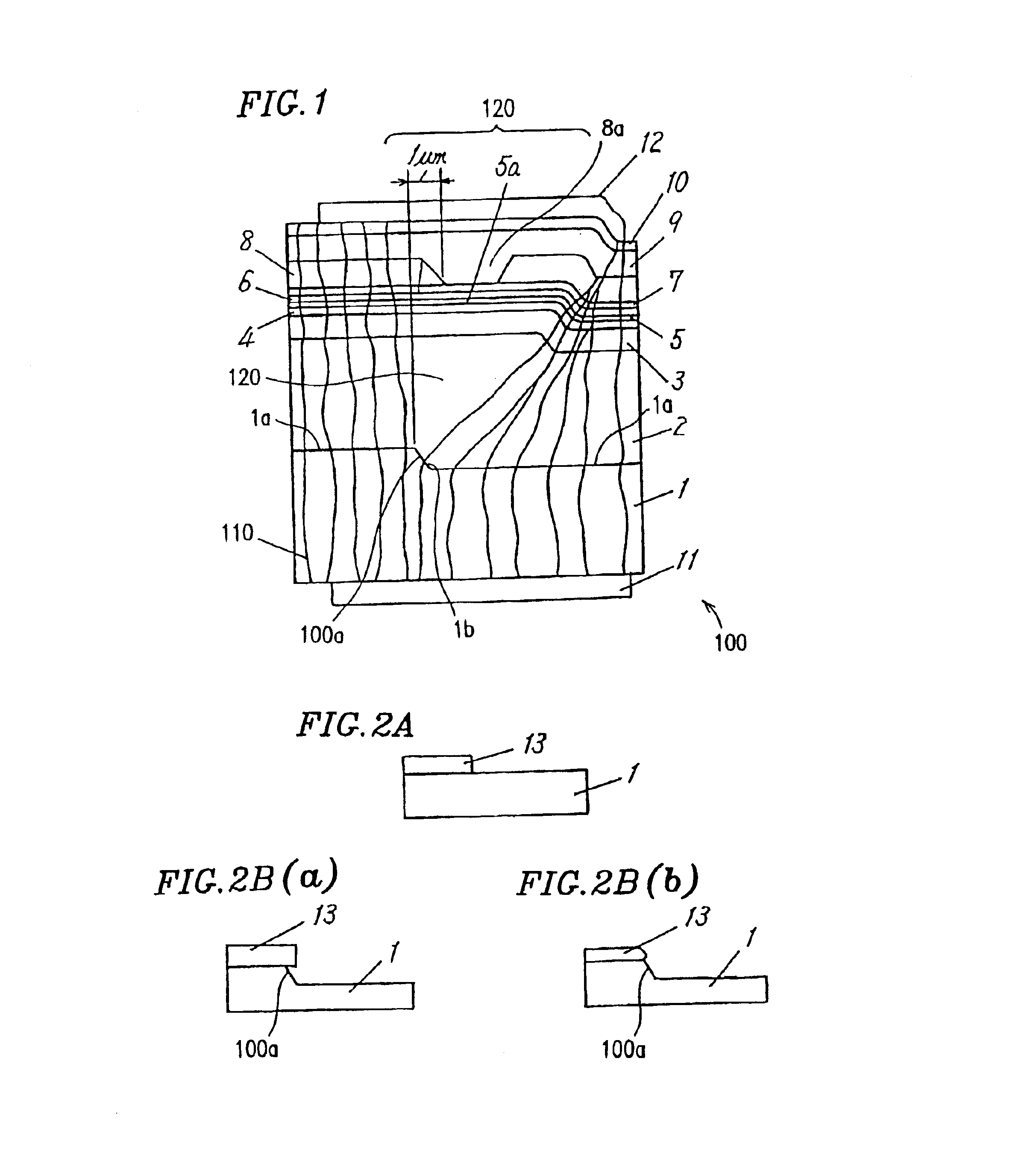
A semiconductor device according to Example 2 of the present invention will be described, along with a fabrication method thereof, with reference to FIGS. 3A through 3F.

As illustrated in FIG. 3A, an AlN layer 14 with a thickness of 5 .mu.m is formed on a (0,0,0,1) sapphire substrate 1 by MOCVD at a temperature of 1000.degree. C. In the AlN layer 14, lattice defects 110 are generated due to a difference in a lattice constant between AlN and sapphire.

As shown in FIG. 3B, a concave and convex structure 14a providing tilted surfaces is then provided for serving as a first stepped configuration on an upper surface of the AlN layer 14 by reactive ion etching. The concave and convex structure 14a has a periodic interval of 10 .mu.m, a width of 2 .mu.m at a top surface of a convex portion (ridge) thereof which has a forward mesa structure, and a depth of 3 .mu.m at a concave portion thereof. A tilted surface of the concave portion of the concave and convex structure 14a extends along a dir...

example 3

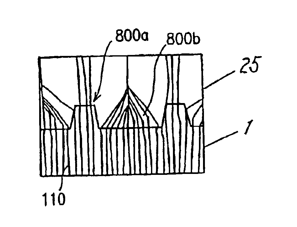
FIG. 5 is a cross-sectional view illustrating a semiconductor device 300 according to Example 3 of the present invention.

A substrate 1 is a hexagonal n-type GaN (0,0,0,1) substrate. Linear lattice defects 110 exist in the substrate 1. A convex portion 300a having tilted surfaces with a surface orientation different from (0,0,0,1) is provided in an upper surface of the substrate 1 so as to provide a concave-and-convex configuration. Thus, the upper surface of the substrate 1 includes a primary surface 1a and the tilted surfaces 1b. The convex portion 300a has a cross section in the shape of a triangle pointing upward from the primary surface 1a of the substrate 1.

An n-type GaN layer 2 with a thickness of 5 .mu.m is formed on the upper surface of the substrate 1. On the n-type GaN layer 2, successively provided are an n-type AlGaN cladding layer 3 with a thickness of 0.5 .mu.m (a mixed crystal ratio of Al to Ga is 10:90), an n-type GaN light guiding layer 4 with a thickness of 0.1 .mu...

example 4

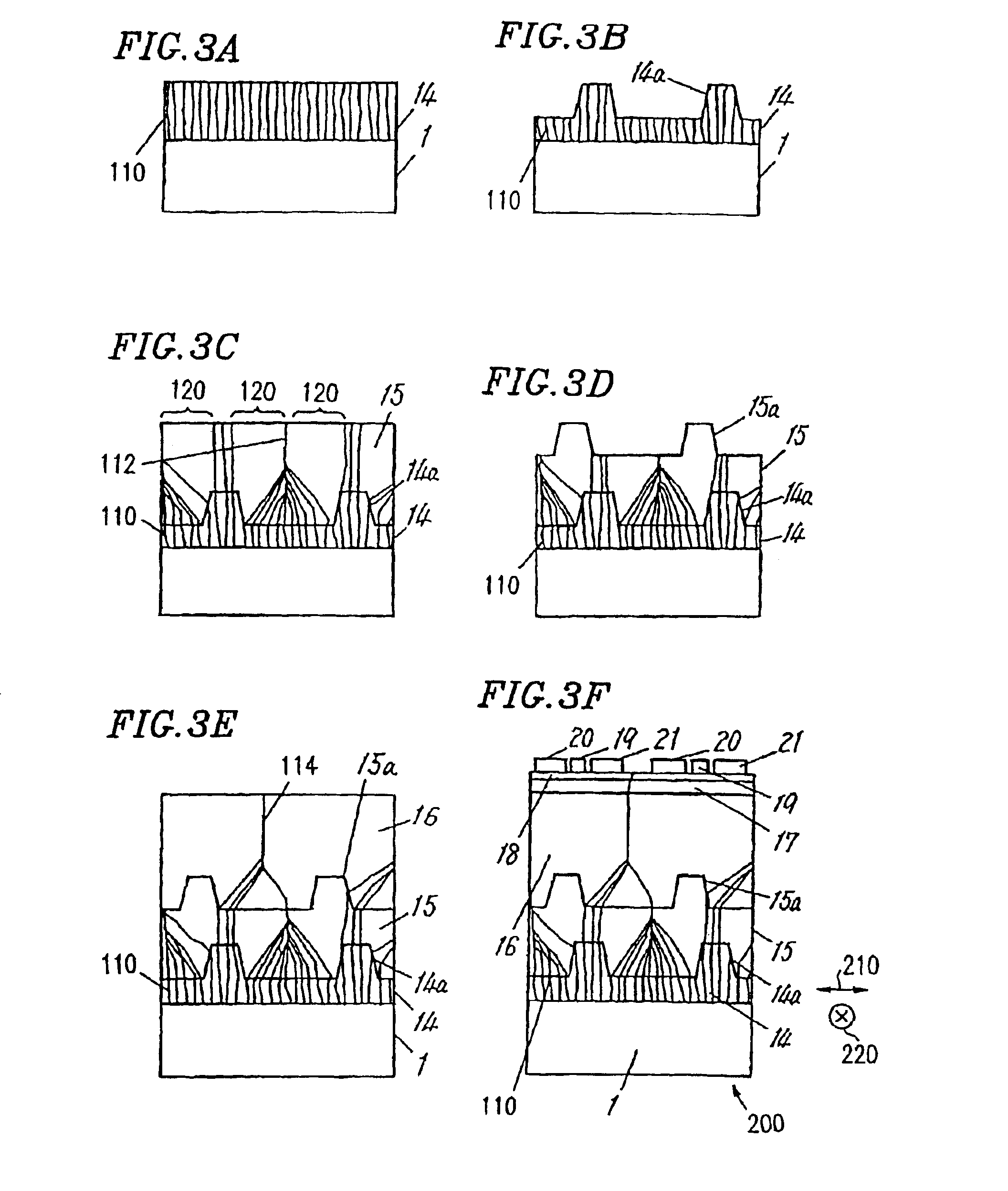
A semiconductor device according to Example 4 of the present invention will be described below, along with a fabrication method thereof, with reference to FIGS. 7A through 7F.

As illustrated in FIG. 7A, an AlN layer 14 with a thickness of 5 .mu.m is formed on a sapphire (0,0,0,1) substrate 1 by MOCVD at a temperature of 1000.degree. C. In the AlN layer 14, linear lattice defects 110 are generated due to a difference in a lattice constant between AlN and Sapphire.

As shown in FIG. 7B, a concave and convex structure 14a providing tilted surfaces is then provided on an upper surface of the AlN layer 14 by reactive ion etching for serving as a first stepped configuration. The tilted surfaces of the concave and convex structure 14a do not have a (0,0,0,1) plane of the AlN layer 14. The tilted surfaces of the concave and convex structure 14a extend along a direction.

As shown in FIG. 7C, a GaN layer 15 with a thickness of 10 .mu.m is formed on the AlN layer 14 by MOCVD. As the GaN layer 15 ...


PUM


Abstract

A semiconductor device includes: a crystalline substrate including a primary surface and a crystal plane provided within the primary surface so as to have a surface orientation different from a surface orientation of the primary surface; a semiconductor layered structure grown over the crystalline substrate; and an active region provided at a portion in the semiconductor layer structure above the crystal plane.

Description

BACKGROUND OF INVENTION1. Field of the InventionThe present invention relates to a semiconductor device, more particularly to a nitride semiconductor device such as a blue laser and a fast-operation transistor, and to a method for fabricating the same. The present invention also relates to a semiconductor substrate and a fabrication method thereof to be used for the above-mentioned semiconductor device and a fabrication method thereof.2. Description of the Related ArtFIG. 4 is a cross sectional view illustrating a conventional semiconductor device 1000. In FIG. 4, a buffer layer 50 is provided on a substrate 1 made of sapphire. On the buffer layer 50, successively provided are an n-type GaN layer 2, an n-type AlGaN cladding layer 3, an n-type GaN light guiding layer 4, an active layer 5 made of i-type InGaN, a p-type GaN light guiding layer 6, a first p-type AlGaN cladding layer 7, a current constriction layer 8 having an opening 8a, a second p-type AlGaN cladding layer 9, and a p-t...

Claims


Application Information

Patent Timeline
Patent Type & Authority Patents(United States)
IPC IPC(8): H01L21/02H01L21/20H01L29/04H01L29/02H01L33/00H01L29/20H01L21/205H01L21/338H01L29/205H01L29/812H01L29/861H01L33/06H01L33/12H01L33/14H01L33/16H01L33/22H01L33/32H01S5/223H01S5/323H01S5/343
CPCH01L21/0237H01L21/0242H01L21/0243H01L21/02433H01L21/02458H01L21/02494H01L21/02502H01L21/0254H01L21/0262H01L21/02658H01L29/045H01L33/007H01L33/0075H01L21/02389H01L33/0079H01L29/2003H01L33/0093
Inventor ISHIDA, MASAHIRONAKAMURA, SHINJIORITA, KENJIIMAFUJI, OSAMUYURI, MASAAKI
Owner XIAMEN SANAN OPTOELECTRONICS CO LTD
Why Eureka
Try Eureka