Field effect transistor

a field effect transistor and transistor technology, applied in the field of normal off-type nitride semiconductor field effect transistors, can solve the problems of low series resistance, affecting the reliability of the element, and the detailed physical properties of the conventional normally-off-type algan/gan mis-hfet involving fluorine implantation, etc., to achieve the effect of low series resistan

Active Publication Date: 2011-06-07
PANASONIC CORP
View PDF3 Cites 46 Cited by
  • Summary
  • Abstract
  • Description
  • Claims
  • Application Information

AI Technical Summary

Benefits of technology

[0014]In order to achieve the above object, a field effect transistor of the invention is formed on a so-called nonpolar plane of a nitride semiconductor. This structure suppresses generation of charges from spontaneous polarization and piezoelectric polarization. Therefore, a normally-off type Group-III nitride semiconductor field effect transistor can be implemented. Moreover, since the nonpolar plane is used as a main surface, increase in sheet carriers in a channel layer from formation of an insulating film can be prevented. Therefore, shift of a threshold voltage to negative bias of the normally-off type field effect transistor can be prevented.
[0016]In the field effect transistor of the invention, the first nitride semiconductor layer has a plane perpendicular to the (0001) plane or a plane tilted with respect to the (0001) plane as a main surface. Therefore, generation of charges from spontaneous polarization and piezoelectric polarization can be suppressed. A normally-off type nitride semiconductor field effect transistor can thus be implemented. Moreover, since a plane perpendicular to the (0001) plane or a plane tilted with respect to the (0001) plane is used as a main surface of the first nitride semiconductor layer, increase in sheet carriers in a channel layer can be prevented when the insulating film is formed between the third nitride semiconductor layer and the gate electrode. Accordingly, reduction in a threshold voltage of the normally-off type field effect transistor can be prevented. Moreover, a normally-off type nitride semiconductor field effect transistor having a higher threshold voltage and excellent operation characteristics can be obtained by using a so-called gate recess structure.
[0018]By doping impurities providing n-type conductivity to the second nitride semiconductor layer, electrons serving as carriers can be supplied to the channel layer of the field effect transistor. Therefore, a series resistance of the transistor can be reduced. By doping impurities providing n-type conductivity to the third nitride semiconductor layer, a contact resistance with an ohmic electrode formed thereon can be reduced. With this structure, a normally-off type field effect transistor having a low series parasitic resistance can be implemented.
[0020]This structure eliminates the need to remove the insulating film by a dry etching method before formation of ohmic electrodes, that is, the source electrode and the drain electrode. Therefore, a normally-off type nitride semiconductor field effect transistor can be obtained without involving damage by plasma processing.
[0022]This improves safety in case of, e.g., power outage and enables operation with a single circuit power supply.

Problems solved by technology

In a conventional Schottky gate structure, however, a significant forward current flows at a gate voltage Vg of about +1 V, and therefore, a gate leakage current flows before a drain current is saturated.
However, detailed physical properties of the conventional normally-off type AlGaN / GaN MIS-HFET involving fluorine implantation have not been clarified.
Moreover, the element is damaged by the plasma processing for fluorine implantation into the AlGaN layer, causing degradation in operation characteristics of the element or fluctuation for reliability through device processing.

Method used


Image

  • Field effect transistor
  • Field effect transistor
  • Field effect transistor

Examples


embodiment

[0044]A field effect transistor according to an embodiment of the invention will now be described with reference to the accompanying drawings. In the following description, an a-plane indicates a (11-20) plane, an r-plane indicates a (1-102) plane, and a c-plane indicates a (0001) plane unless otherwise mentioned. For convenience, a negative sign given to a Miller index of plane orientation indicates inversion of an index following the negative sign.

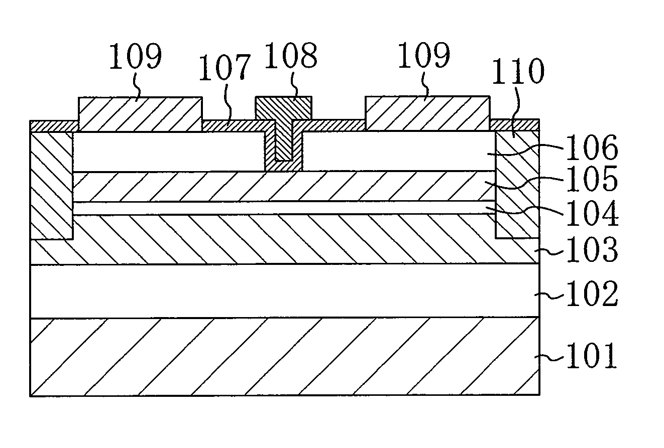
[0045]FIG. 1 shows a cross-sectional structure of an AlGaN / GaN heterojunction field effect transistor having an a-plane as a main surface (hereinafter, simply referred to as an a-plane AlGaN / GaN HFET) according to a first embodiment of the invention.

[0046]As shown in FIG. 1, for example, an AlN (aluminum nitride) buffer layer 102 having a thickness of 500 nm, an undoped GaN layer 103 having a thickness of 3 nm, an AlN spacer layer 104 having a thickness of 1 nm, an n-type AlxGa1-xN barrier layer 105 (0106 having a thickness of 50 nm are ...


PUM


Abstract

A field effect transistor includes: a first nitride semiconductor layer having a plane perpendicular to a (0001) plane or a plane tilted with respect to the (0001) plane as a main surface; a second nitride semiconductor layer formed on the first nitride semiconductor layer and having a wider bandgap than the first nitride semiconductor layer; a third nitride semiconductor layer formed on the second nitride semiconductor layer; and a source electrode and a drain electrode formed so as to contact at least a part of the second nitride semiconductor layer or the third nitride semiconductor layer. A recess that exposes a part of the second nitride semiconductor layer is formed between the source electrode and the drain electrode in the third nitride semiconductor layer. A gate electrode is formed in the recess and an insulating film is formed between the third nitride semiconductor layer and the gate electrode.

Description

CROSS REFERENCE TO RELATED APPLICATION[0001]This application claims priority under 35 U.S.C. §119 on Patent Application No. 2007-111451 filed in Japan on Apr. 20, 2007, the entire contents of which are hereby incorporated by reference.BACKGROUND OF THE INVENTION[0002]1. Field of the Invention[0003]The invention relates to a normally-off type nitride semiconductor field effect transistor that is used in a high breakdown voltage power transistor.[0004]2. Background Art[0005]A GaN (gallium nitride) based compound semiconductor has a high breakdown field and a high saturation electron velocity and therefore is a very attractive semiconductor material for a future power transistor that requires a low on-state resistance and a high breakdown voltage. In an AlGaN / GaN (aluminum gallium nitride / gallium nitride) heterostructure formed on a substrate having a (0001) plane as a main surface, charges are formed at the heterointerface by spontaneous polarization and piezoelectric polarization, an...

Claims


Application Information

Patent Timeline
Patent Type & Authority Patents(United States)
IPC IPC(8): H01L31/072H01L21/338H01L29/778H01L29/812
CPCH01L29/7787H01L29/66462H01L29/42376H01L29/045H01L29/2003H01L29/4236H01L29/452H01L29/518
Inventor KURODA, MASAYUKIUEDA, TETSUZO
Owner PANASONIC CORP
Why Eureka
Try Eureka