Field effect transistor structure

a field effect transistor and transistor structure technology, applied in the field of semiconductor devices, can solve the problems of reducing drain current and difficult manufacturing, and achieve the effects of reducing low-frequency noise (lfn), high on/off current ratio, and high threshold voltage modulation

Active Publication Date: 2017-11-02
NAT CHIAO TUNG UNIV
View PDF1 Cites 3 Cited by
  • Summary
  • Abstract
  • Description
  • Claims
  • Application Information

AI Technical Summary

Benefits of technology

[0005]The disclosure provides an FET structure that can prevent the issue of the roll-off of a threshold voltage and is characterized by a negligible drain-induced barrier lowering (DIBL), the sub-threshold slope (SS) approximating to an ideal value, a high on / off current ratio, high threshold voltage modulation, reduced low-frequency noise (LFN), good reliability, low current leakage, small series resistance, and reduced current crowding effects.

Problems solved by technology

Nevertheless, it is difficult to manufacture the JL FET, and the overly high source / drain (S / D) series resistance may lead to the decrease in the drain current.
Therefore, how to achieve satisfactory electrical performance and simultaneously simplify the manufacturing process has become one of the challenges that the manufacturers face.

Method used


Image

  • Field effect transistor structure
  • Field effect transistor structure
  • Field effect transistor structure

Examples


first embodiment

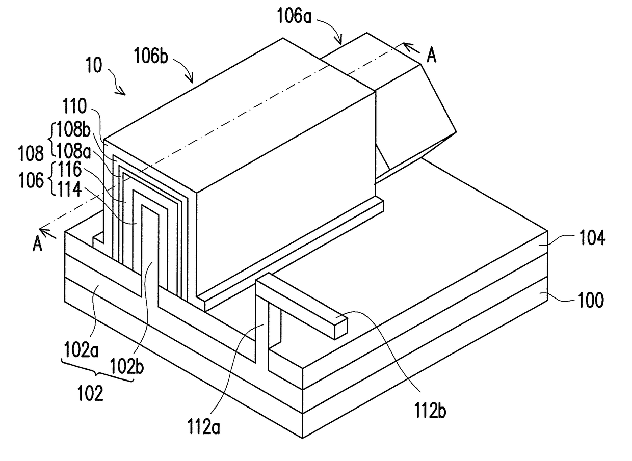
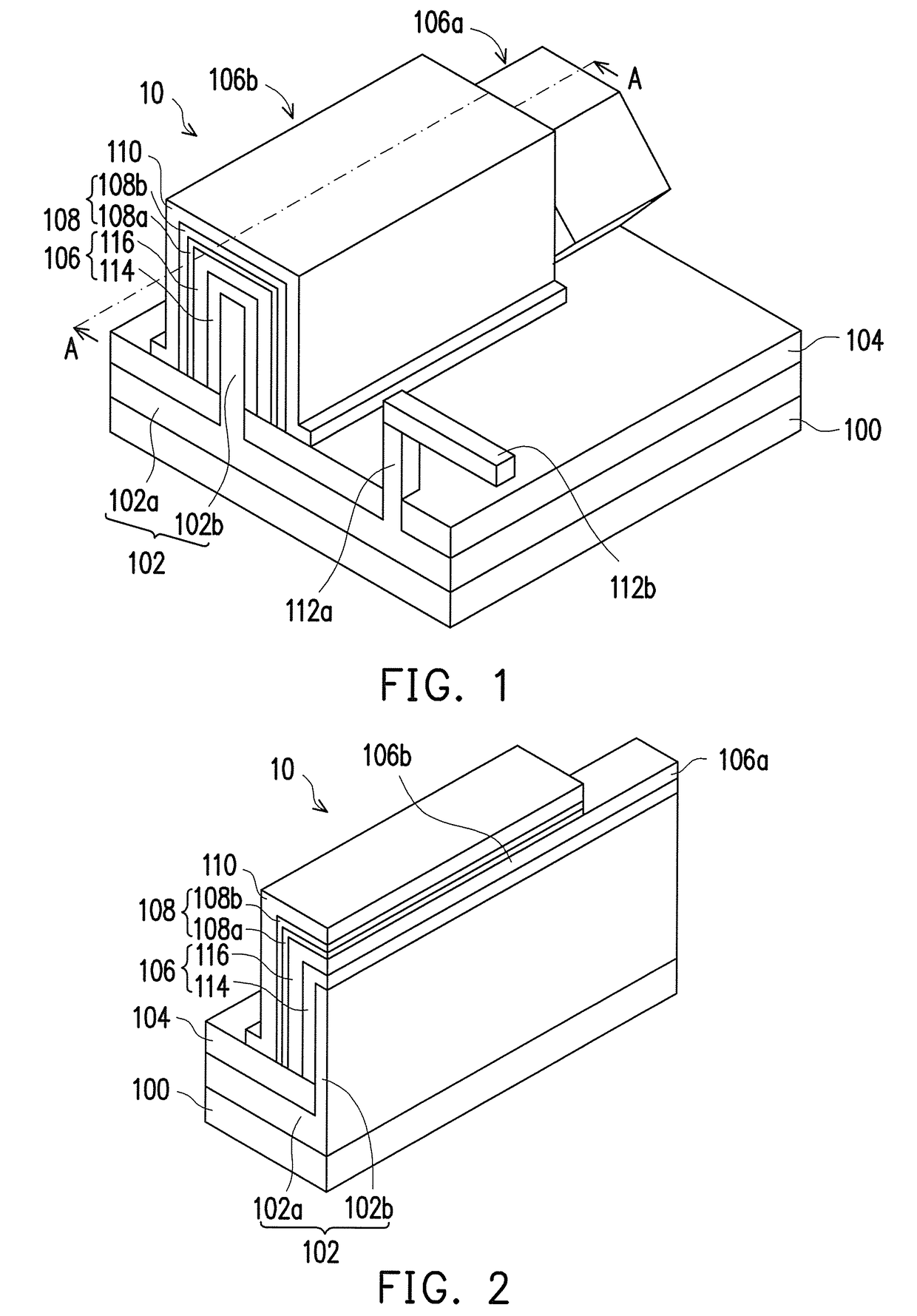
[0037]FIG. 1 is a schematic three-dimensional view illustrating an FET structure according to the disclosure. FIG. 2 is a schematic three-dimensional view taken along a section line A-A depicted in FIG. 1.

[0038]With reference to FIG. 1 and FIG. 2, an FET structure 10 provided in the first embodiment includes a substrate 100, an internal gate 102, an insulation layer 104, a semiconductor strip 106, a gate dielectric insulator 108, and a gate conductor 110. The internal gate 102 includes a floor portion 102a located on the substrate 100 and a wall portion 102b extending from the floor portion 102a. The insulation layer 104 is located on the floor portion 102a of the internal gate 102. The semiconductor strip 106 is located on the wall portion 102b and a portion of the insulation layer 104, and the semiconductor strip 106 includes source / drain regions 106a and a channel region 106b adjacent to the source / drain regions 106a. The gate dielectric insulator 108 is located on the channel re...

second embodiment

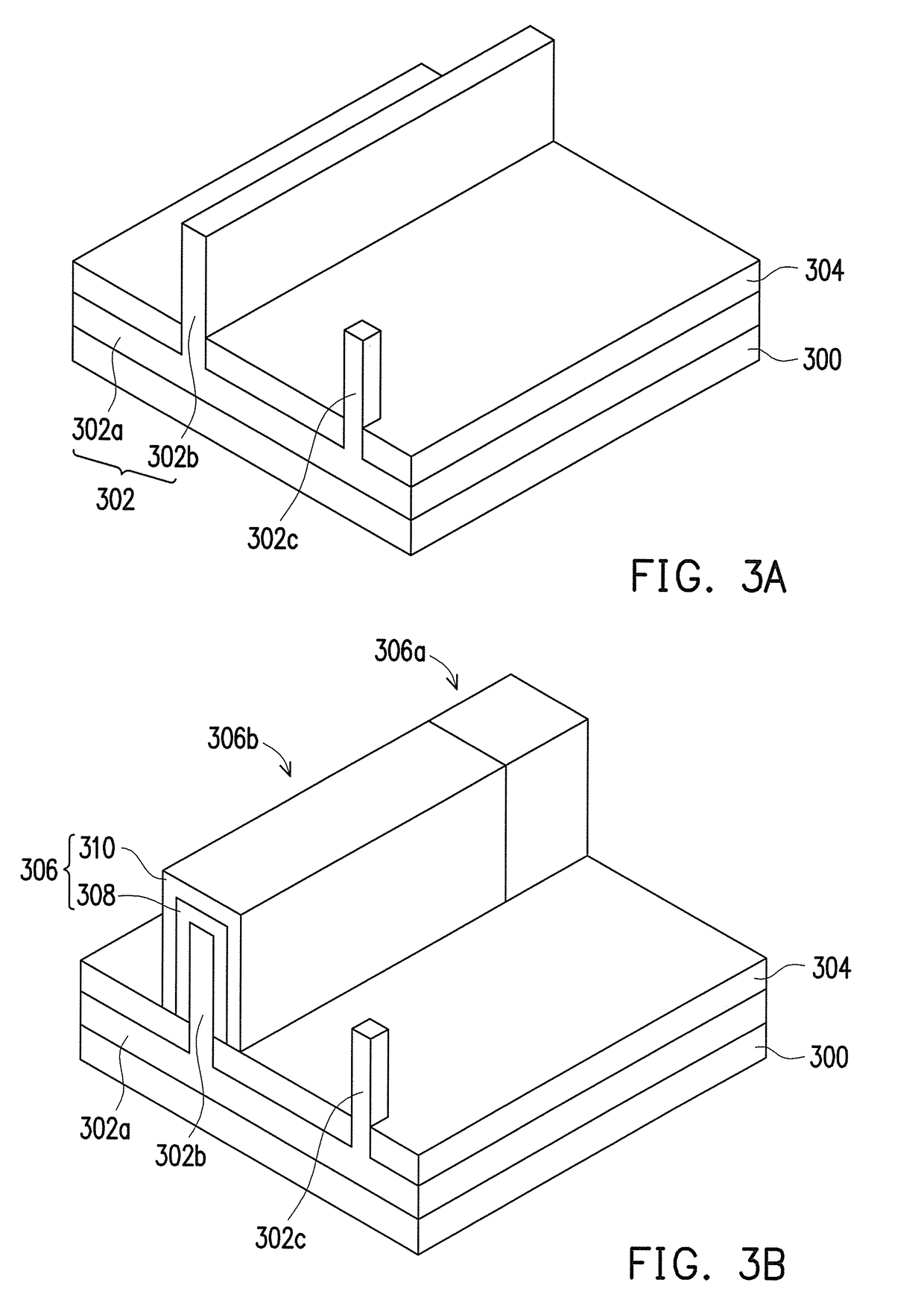
[0051]FIG. 3A to FIG. 3E are schematic views illustrating a manufacturing process of an FET structure according to the disclosure.

[0052]With reference to FIG. 3A, an internal gate 302 is formed on a substrate 300 through performing an epitaxial growing process and a photolithography and etching process. The internal gate 302 includes a floor portion 302a, a wall portion 302b, and a contact pillar 302c. The contact pillar 302c and the internal gate 302 belong to the same structure. A deposition process and a dry etching process are performed, so as to form an insulation layer 304 on the floor portion 302a of the internal gate 302, and the wall portion 302b and the contact pillar 302c are exposed.

[0053]With reference to FIG. 3B, an epitaxial growing process is performed to sequentially form a first semiconductor layer 308 and a second semiconductor layer 310 of a semiconductor strip 306. The semiconductor strip 306 includes source / drain regions 306a and a channel region 306b adjacent ...

sixth embodiment

[0063]FIG. 8A to FIG. 8E are schematic views illustrating a manufacturing process of an FET structure according to the disclosure.

[0064]With reference to FIG. 8A, an internal gate 802 is formed on a substrate 800 through performing an epitaxial growing process and a photolithography and etching process. The internal gate 802 includes a floor portion 802a, a wall portion 802b, and a contact pillar 802c. The contact pillar 802c and the internal gate 802 belong to the same structure. A deposition process and a dry etching process are performed, so as to form an insulation layer 804 on the floor portion 802a and the wall portion 802b of the internal gate 802, and the contact pillar 802c is exposed.

[0065]In the present embodiment, the wall portion 802b of the internal gate 802 is substantially formed on a location where the channel region 806b is to be formed, and the wall portion 802b does not extend to the location where the source / drain regions 806a are to be formed. Hence, it is expe...


PUM


Abstract

A field effect transistor (FET) structure includes a substrate, an internal gate, an insulation layer, a semiconductor strip, a gate dielectric insulator, and a gate conductor. The internal gate includes a floor portion located on the substrate and a wall portion extending from the floor portion. The insulation layer is located on the floor portion of the internal gate. The semiconductor strip is located on the wall portion and a portion of the insulation layer, and the semiconductor strip includes source/drain regions and a channel region adjacent to the source/drain regions. The gate dielectric insulator is located on the channel region. The gate conductor is located on the gate dielectric insulator.

Description

CROSS-REFERENCE TO RELATED APPLICATION[0001]This application claims the priority benefit of Taiwan application serial no. 105113196, filed on Apr. 28, 2016. The entirety of the above-mentioned patent application is hereby incorporated by reference herein and made a part of this specification.TECHNICAL FIELD[0002]The disclosure relates to a semiconductor device, and more particularly, to a field effect transistor (FET) structure.DESCRIPTION OF RELATED ART[0003]In recent years, due to the requirement for the miniaturization of transistors, various manufacturing technologies have developed. Here, the junctionless (JL) field effect transistor (FET) that can effectively lessen the impact of short channel effect (SCE) and parasitic series resistance has been considered as one of the mainstream products.[0004]Nevertheless, it is difficult to manufacture the JL FET, and the overly high source / drain (S / D) series resistance may lead to the decrease in the drain current. Therefore, how to achi...

Claims


Application Information

Patent Timeline
Patent Type & Authority Applications(United States)
IPC IPC(8): H01L51/05H01L51/10H01L27/28H01L51/00
CPCH01L51/0554H01L51/0562H01L51/0516H01L51/102H01L27/0886H01L51/0021H01L51/107H01L51/0529H01L27/283H01L29/7831H01L2029/7857H10K85/113H10K10/474H10K10/471H10K10/481H10K10/482H10K10/486H10K10/484H10K10/88H10K10/82H10K10/468H10K19/10H10K71/60
Inventor CHANG, CHUN-YEN
Owner NAT CHIAO TUNG UNIV
Why Eureka
Try Eureka