Method for forming dielectric film using siloxane-silazane mixture

a technology of siloxane and siloxane, which is applied in the field of siloxane-containing dielectric films, can solve the problems of film's resistance to damascene processing technology to deteriorate significantly, reduce the film density too much, and achieve high density and high strength. , the effect of high density

Active Publication Date: 2009-06-18
ASM JAPAN
View PDF19 Cites 204 Cited by
  • Summary
  • Abstract
  • Description
  • Claims
  • Application Information

AI Technical Summary

Benefits of technology

[0012]To solve one or more of the aforementioned problems, an embodiment of the present invention provides a method for forming a low dielectric constant film by mixing a silicon-containing hydrocarbon gas and a silazane-containing gas to achieve a low dielectric film having high density and high strength. In an embodiment, the formed film has Si—O, Si—CH3, Si—H, C—H, Si—N and N—H bonds, and thus treating the film under heat and through UV curing in an atmosphere of oxidizing gas replaces Si—N and Si—H with Si—O and the final film only has Si—O, Si—CH3 and C—H bonds. ...

Problems solved by technology

However, lowering the dielectric constant promotes density reduction, resulting in the film sustaining significant damage in the etching, ashing and other steps in the damascene process.
However, it lowers the film density too much and causes the film's resistance to the damascene processing technology to deteriorate significantly.
Although these films achieve a dielectric constant of 2 or even less, inclusion of boron in the composition presents concerns over insulation performance.
In particular, these films tend to lose resistance over time.
Significant changes to the processing schemes using conventional silicon oxide films increased the time needed to start mass production, because improving the processing scheme to prevent damage caused by lower mechanical strength took longer ...

Method used


Image

  • Method for forming dielectric film using siloxane-silazane mixture
  • Method for forming dielectric film using siloxane-silazane mixture
  • Method for forming dielectric film using siloxane-silazane mixture

Examples


example

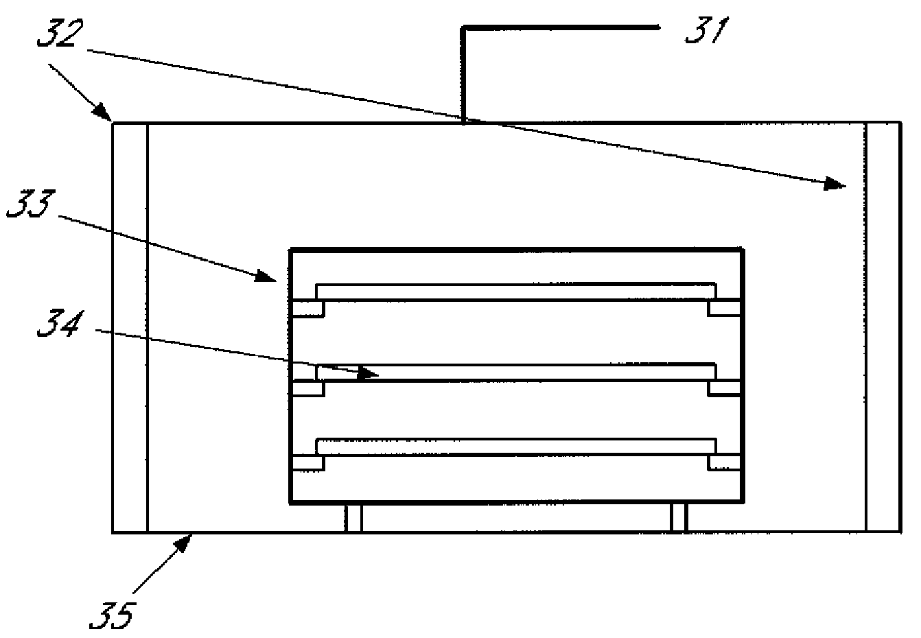
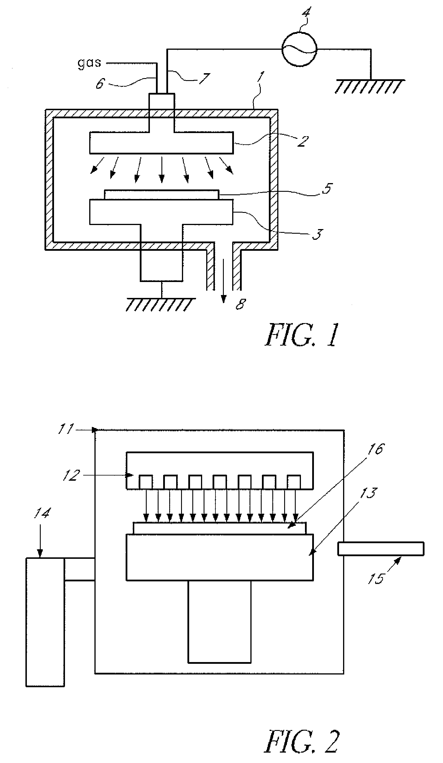
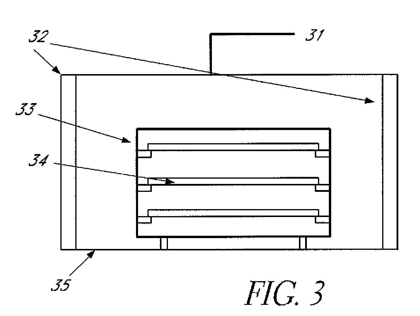
[0059]Specific examples are explained below. Low dielectric constant films were formed using the apparatus shown in FIG. 1 under the conditions specified in Table 1.

TABLE 1Film Forming ConditionsM-DischargeSusceptorTMOS1.1.3.3TMDSHe13.56 MHzPressuregapHeatXe-UVExample(° C.)(sccm)(sccm)(sccm)(W)(Pa)(mm)treatmenttreatment120252560025040024400° C.400° C. O2O2 / N22↓5025↓↓↓↓↓↓3↓2550↓↓↓↓↓↓4−55025400300↓28↓↓5↓100↓↓↓↓↓↓↓6↓200↓↓↓↓↓↓↓M-TMOS: Methyl trimethoxysilane1,1,3,3 TMDS: 1,1,3,3 tetramethyl disilazane

TABLE 2Evaluation Results of Film Quality CharacteristicsDielectricDielectricbreakdownLeak currentEMFilm densityN groups in filmEmbeddingExampleconstant(MV)2 MV(A / cm2)(GPa)(g / cm3)(%)characteristics12.65.51.0E−9151.4Not detectedFavorablecharacteristics22.55.33.1E−9141.36↓↓32.75.72.1E−9181.43↓↓42.45.25.8E−9131.34↓↓52.25.25.2E−9121.3↓↓62.05.14.3E−9101.25↓↓Film density: Measured result using XRR / Remaining N groups in film: Measured by RBS-HFS

[0060]The film forming time was set so as to achieve ...


PUM

PropertyMeasurementUnit
Temperatureaaaaaaaaaa
Wavelengthaaaaaaaaaa

Abstract

A method of forming a dielectric film, includes: introducing a siloxane gas essentially constituted by Si, O, C, and H and a silazane gas essentially constituted by Si, N, H, and optionally C into a reaction chamber where a substrate is placed; depositing a siloxane-based film including Si—N bonds on the substrate by plasma reaction; and annealing the siloxane-based film on the substrate in an annealing chamber to remove Si—N bonds from the film.

Description

BACKGROUND OF THE INVENTION [0001]1. Field of the Invention[0002]The present invention relates generally to a semiconductor technique and more particularly to a silicone-containing dielectric film having good mechanical strength.[0003]2. Description of the Related Art[0004]In the plasma chemical vapor deposition (plasma CVD) method, a film is formed on a semiconductor substrate by placing the semiconductor substrate, being the processing target, on a heater of resistance heating type, etc., that has been heated to a temperature of 0 to 350° C. in an atmosphere of 1 to 10 Torr. The heater is installed in a manner facing a shower plate that releases a reactant gas, and RF power of 13.56 to 60 MHz, etc., is applied to the shower plate at an output of 100 to 4,000 W to implement RF discharge between the heater and shower plate and thereby generate plasma. This plasma CVD method is used to form thin films such as inter-layer insulation films, passivation films and anti-glare films.[0005]...

Claims


Application Information

Patent Timeline
IPC IPC(8): H01L21/31
CPCC23C16/401C23C16/56H01L21/02126H01L21/02216H01L21/02222H01L21/02274H01L21/31612H01L21/02337H01L21/02348H01L21/3105H01L21/3122H01L21/3125H01L21/02315
Inventor FUKAZAWA, ATSUKILEE, WOO JINMATSUKI, NOBUO
Owner ASM JAPAN
Why Eureka
Try Eureka