METHOD OF MANUFACTURING ZnO SEMICONDUCTOR LAYER FOR ELECTRONIC DEVICE AND THIN FILM TRANSISTOR INCLUDING THE ZnO SEMICONDUCTOR LAYER

Inactive Publication Date: 2008-11-13
ELECTRONICS & TELECOMM RES INST
View PDF1 Cites 192 Cited by
  • Summary
  • Abstract
  • Description
  • Claims
  • Application Information

AI Technical Summary

Benefits of technology

[0012]The present invention is directed to a method of manufacturing a ZnO semiconductor layer for an electronic device in which much larger c

Problems solved by technology

Also, since deposited transparent semiconductors are subject to a high-temperature thermal treatment process, scaling up the transparent semiconductors is difficult and the transparent TFTs are inferior in terms of performance to a-Si TFTs.
Furthermore, because manufacturing the transparent TFTs is costly, the transparent TFTs are inadequate for ubiquitous environments requiring low-priced TFTs.
However, since the OTFTs have poorer performance than conventional TFTs, applying the OTFTs to typical electronic devices is not easy.
Also, organic semiconducto

Method used


Image

  • METHOD OF MANUFACTURING ZnO SEMICONDUCTOR LAYER FOR ELECTRONIC DEVICE AND THIN FILM TRANSISTOR INCLUDING THE ZnO SEMICONDUCTOR LAYER
  • METHOD OF MANUFACTURING ZnO SEMICONDUCTOR LAYER FOR ELECTRONIC DEVICE AND THIN FILM TRANSISTOR INCLUDING THE ZnO SEMICONDUCTOR LAYER
  • METHOD OF MANUFACTURING ZnO SEMICONDUCTOR LAYER FOR ELECTRONIC DEVICE AND THIN FILM TRANSISTOR INCLUDING THE ZnO SEMICONDUCTOR LAYER

Examples


Embodiment Construction

[0024]The present invention will now be described more fully hereinafter with reference to the accompanying drawings, in which exemplary embodiments of the invention are shown.

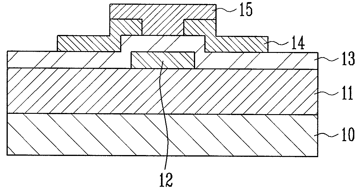
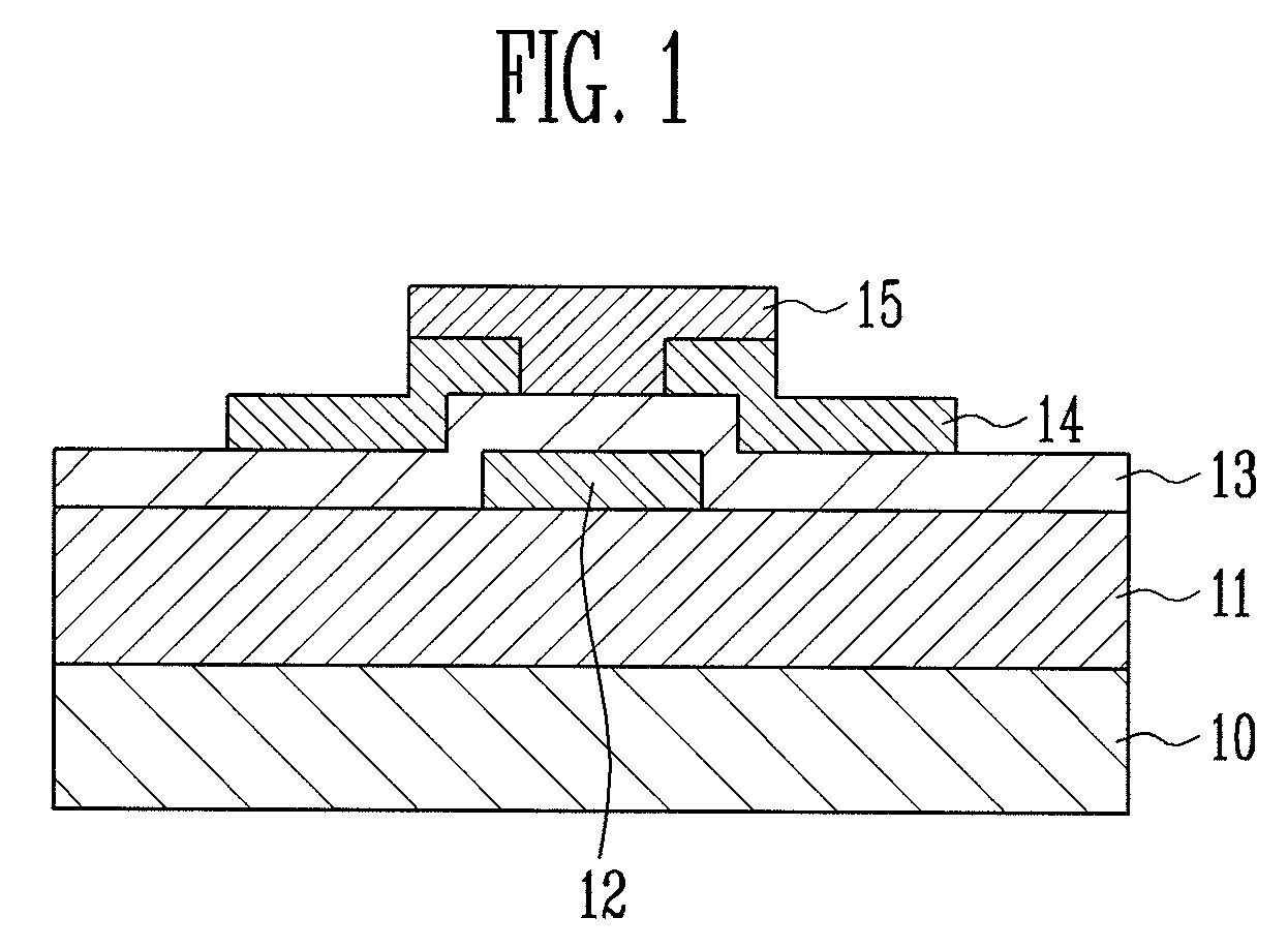
[0025]FIG. 1 is a cross-sectional view of a thin film transistor (TFT) including a semiconductor layer manufactured according to an exemplary embodiment of the present invention.

[0026]Referring to FIG. 1, a TFT 1 includes a substrate 10, an insulating layer 11 disposed on the substrate 10, a gate electrode 12 disposed on the insulating layer 11, a gate insulating layer 13 disposed on the gate electrode 12, source and drain electrodes 14 disposed on the gate insulating layer 13, and a semiconductor layer 15 disposed on the gate insulating layer 13 to contact the source and drain electrodes 14.

[0027]The substrate 10 may be formed of various materials, such as glass, silicon, metal foil such as stainless steel (SUS), and plastic. When manufacturing a TFT using a transparent substrate, a transparent display device...


PUM


Abstract

Provided are a method of manufacturing a ZnO semiconductor layer for an electronic device, which can control the size of crystals of the ZnO semiconductor layer and the number of carriers using a surface chemical reaction between precursors, and a thin film transistor (TFT) including the ZnO semiconductor layer. The method includes: (a) loading a substrate into a chamber; (b) injecting a Zn precursor into the chamber to adsorb the Zn precursor on the substrate; (c) injecting an inert gas or N2 gas into the chamber to remove the remaining Zn precursor; (d) injecting an oxygen precursor into the chamber to cause a reaction between the oxygen precursor and the Zn precursor adsorbed on the substrate to form the ZnO semiconductor layer; (e) injecting the N2 gas or inert gas into the chamber to remove the remaining oxygen precursor; (f) repeating steps (a) through (e); (g) repeatedly processing the surface treatment of the ZnO semiconductor layer using O2 plasma or O3; (h) injecting the N2 gas or inert gas into the chamber to remove the remaining oxygen and Zn precursors; and (i) repeating steps (a) through (h) to control the thickness of the ZnO semiconductor layer. In this method, a transparent TFT is formed using a transparent substrate to enable manufacture of a transparent display device, and a flexible display device can be manufactured using a flexible substrate. Also, the crystallinity of the ZnO semiconductor layer can be increased to improve the mobility of a TFT, and the number of carriers can be controlled to reduce a leakage current. Therefore, a ZnO semiconductor having excellent characteristics can be manufactured.

Description

CROSS-REFERENCE TO RELATED APPLICATION[0001]This application claims priority to and the benefit of Korean Patent Application Nos. 2007-2525, filed Jan. 9, 2007 and 2007-51792, filed May 29, 2007, the disclosures of which are incorporated herein by reference in their entirety.BACKGROUND[0002]1. Field of the Invention[0003]The present invention relates to a method of manufacturing a Zinc Oxide (ZnO) semiconductor layer for an electronic device and, more particularly, to a method of manufacturing a ZnO semiconductor layer for an electronic device by causing a surface chemical reaction between an oxygen precursor and a Zn precursor using an Atomic Layer Deposition (ALD) technique, and a thin film transistor (TFT) including the ZnO semiconductor layer.[0004]The present invention has been produced from the work supported by the IT R&D program of MIC (Ministry of Information and Communication) / IITA (Institute for Information Technology Advancement) [2006-S-079-01, Smart window with transpa...

Claims


Application Information

Patent Timeline
IPC IPC(8): H01L21/20H01L29/786
CPCH01L21/0237H01L21/02488H01L29/66969H01L21/0262H01L29/7869H01L21/02554
Inventor PARK, SANG HEEHWANG, CHI SUNCHU, HYE YONGLEE, JEONG IK
Owner ELECTRONICS & TELECOMM RES INST
Why Eureka
Try Eureka