Semiconductor device

a technology of semiconductor materials and devices, applied in the direction of semiconductor devices, basic electric elements, electrical apparatus, etc., can solve the problems of increasing the size of the smallest components, increasing the difficulty of achieving the effect of enhancing the electric field, and increasing the complexity of the circui

Active Publication Date: 2018-01-16
UNITED MICROELECTRONICS CORP
View PDF11 Cites 5 Cited by
  • Summary
  • Abstract
  • Description
  • Claims
  • Application Information

AI Technical Summary

Benefits of technology

[0009]According to the semiconductor devices provided by the present invention, the tri-layered gate-control stack is provided between the electrode layer and the substrate, and the tri-layered gate-control stack includes the FE layer, the AFE layer and the mid-gap metal layer. It is noteworthy that in the tri-layered gate-control stack, the mid-gap metal layer is always sandwiched between the FE layer and the substrate while the AFE layer is disposed on or under the dual-layered structure consisting of the FE layer and the mid-gap metal layer. The FE layer is provided to enhance electric fields created by the electrode layer and the mid-gap metal layer is provided to homogenize the enhanced electric fields. Furthermore, the AFE layer is provided to render negative capacitance effect. The tri-layered gate-control stack is therefore used to replace conventional high-k gate dielectric layer according to the present invention, and the semiconductor device provided by the present invention therefore obtains smaller subthreshold swing.

Problems solved by technology

Since the semiconductor integrated circuit industry has experienced rapid growth and improvement, technological advances in semiconductor materials and design have produced increasingly smaller and more complex circuits.
However, as the size of the smallest components has decreased, numerous challenges have risen.
As features become closer, current leakage can become more noticeable, signals can crossover more easily, and power usage has become a significant concern.
However, the subthreshold swing cannot be less than 60 mV / sec due to the physical limit of MOS FET device in state-of-the-art.

Method used


Image

  • Semiconductor device
  • Semiconductor device
  • Semiconductor device

Examples


Embodiment Construction

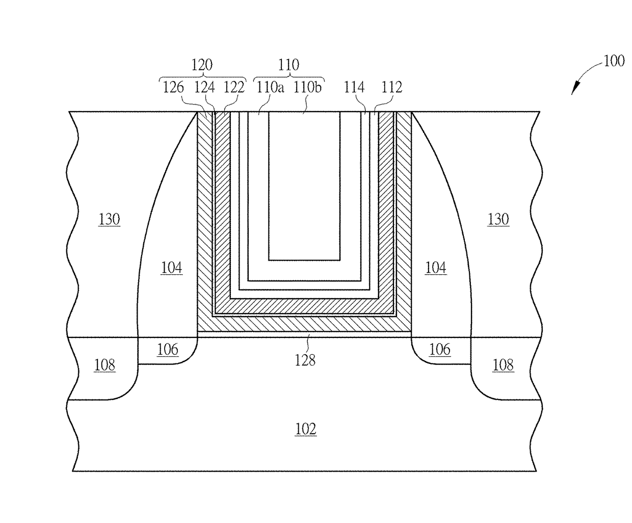
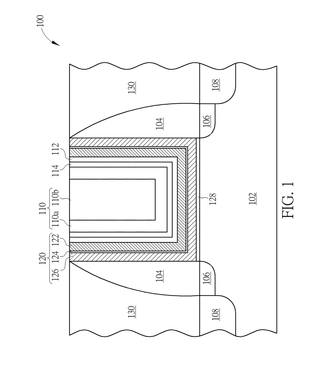
[0013]Please refer to FIG. 1, which is a schematic drawing illustrating a semiconductor device provided by a first preferred embodiment of the present invention. As shown in FIG. 1, a semiconductor device 100 is proved by the preferred embodiment, and the semiconductor device 100 includes a substrate 102 such as silicon substrate, silicon-containing substrate, or silicon-on-insulator (hereinafter abbreviated as SOI) substrate. A plurality of isolation structures (not shown) is formed in the substrate 102. The isolation structures can be shallow trench isolations (STIs), but not limited to this. The isolation structures are used to define a plurality of active regions for accommodating p-typed FET (hereinafter abbreviated as pFET) devices and / or n-typed FET (hereinafter abbreviated as nFET) devices, and to provide electrical isolation. In some preferred embodiments of the present invention, a semiconductor layer such as a fin structure involved in fin field effect transistor (FinFET)...


PUM

PropertyMeasurementUnit
work functionaaaaaaaaaa
ferroelectricaaaaaaaaaa

Abstract

A semiconductor device includes a substrate, an electrode layer disposed on the substrate, and a tri-layered gate-control stack sandwiched between the substrate and the electrode layer. The tri-layered gate-control stack includes a ferroelectric layer disposed on the substrate, a mid-gap metal layer sandwiched between the ferroelectric layer and the substrate, and an anti-ferroelectric layer. The anti-ferroelectric layer is sandwiched between the substrate and the mid-gap metal layer. Alternatively, the ferroelectric layer and the mid-gap metal layer are sandwiched between the anti-ferroelectric layer and the substrate.

Description

BACKGROUND OF THE INVENTION[0001]1. Field of the Invention[0002]The present invention relates to a semiconductor device, and more particularly, to a semiconductor device including ferroelectric (hereinafter abbreviated as FE) material and anti-ferroelectric (hereinafter abbreviated as AFE) material.[0003]2. Description of the Prior Art[0004]A semiconductor device means any device which can function by utilizing semiconductor characteristics, such as an electro-optical device, a semiconductor circuit, and an electronic device. Accordingly, semiconductor devices are used in a variety of electronic applications, such as personal computers, cell phones, digital cameras, and other electronic equipment, as example.[0005]Semiconductor devices are typically fabricated by sequentially depositing insulating or dielectric layer, conductive layers, and semiconductor layers over a semiconductor substrate, and patterning the various material layers using lithography to form circuit components and...

Claims


Application Information

Patent Timeline
Patent Type & Authority Patents(United States)
IPC IPC(8): H01L29/78H01L29/51H01L29/49H01L29/66
CPCH01L29/78391H01L29/4966H01L29/6684H01L29/517H01L29/516H01L29/40111
Inventor CHEN, SHIH-CHENGWEN, TSAI-YUYE, SHANLU, TSUO-WEN
Owner UNITED MICROELECTRONICS CORP
Why Eureka
Try Eureka