Methods for manufacturing thin film transistor and display device

a thin film transistor and display device technology, applied in semiconductor/solid-state device manufacturing, semiconductor devices, electrical equipment, etc., can solve the problems of reducing yield, difficult to remove the resist mask with phenol, chlorobenzene, leakage current, etc., to improve the contrast ratio of the display device, improve the effect of subthreshold swing and excellent switching characteristics

Inactive Publication Date: 2010-03-11
SEMICON ENERGY LAB CO LTD
View PDF29 Cites 17 Cited by
  • Summary
  • Abstract
  • Description
  • Claims
  • Application Information

AI Technical Summary

Benefits of technology

[0044]A thin film transistor of one embodiment of the present invention has a small subthreshold swing and excellent switching characteristics. Thus, if the thin film transistor is employed for a display device, the contrast ratio of the display device can be improved and the power consumption can be reduced. Moreover, because variation in electric characteristics between elements is small, a display device with less display unevenness can be provided.
[0045]Accordingly, by employing a thin film transistor of one embodiment of the present invention for a display device, the image quality of the display device can be improved.

Problems solved by technology

A substance included in the remover solution or a residue of the remaining resist mask exists in a back channel portion or the like, which causes leakage current.
However, it is difficult to remove the resist mask with phenol, chlorobenzene, or the like alone in many cases, and the photoresist mask that cannot be removed causes reduction in yield.

Method used


Image

  • Methods for manufacturing thin film transistor and display device
  • Methods for manufacturing thin film transistor and display device
  • Methods for manufacturing thin film transistor and display device

Examples


embodiment 1

[0094]In this embodiment, a method for manufacturing a thin film transistor which is one embodiment of the present invention and the thin film transistor manufactured by the method will now be described with reference to drawings.

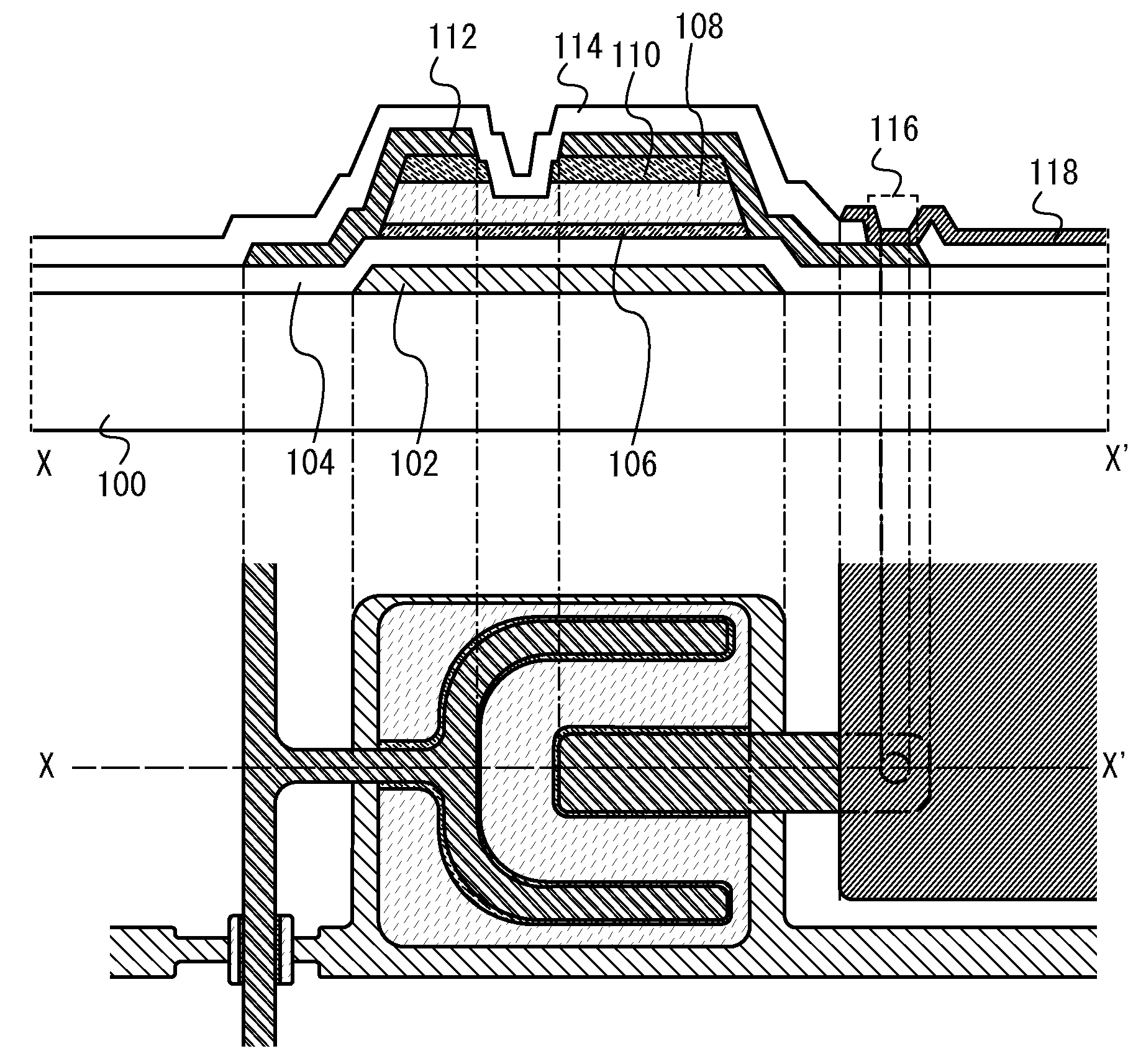
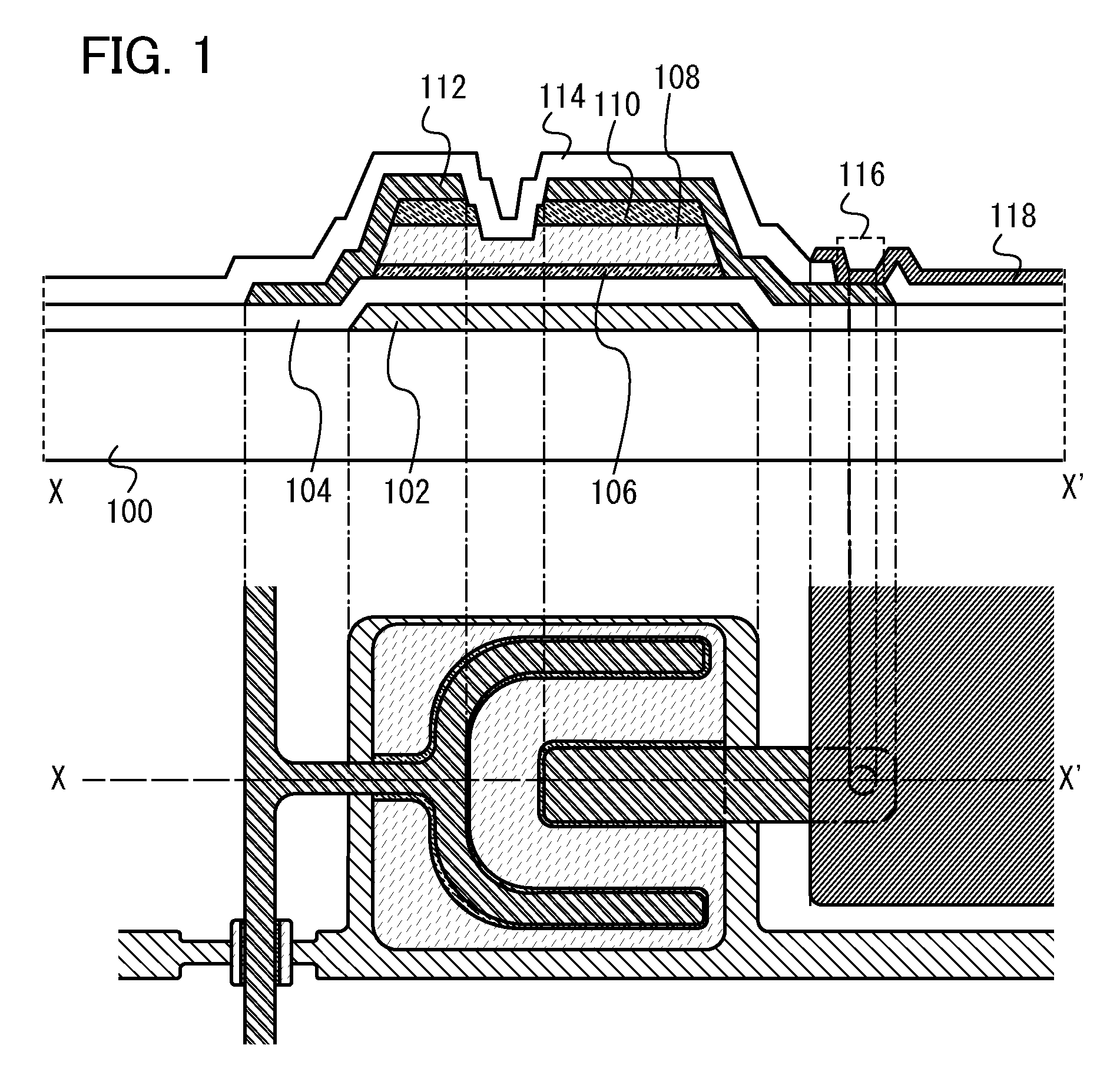
[0095]FIG. 1 illustrates a top view and a cross-sectional view of a thin film transistor which is one embodiment of the present invention as an example. The thin film transistor illustrated in FIG. 1 includes a gate electrode layer 102 over a substrate 100, a gate insulating layer 104 over the gate electrode layer 102, a semiconductor layer 106 over the gate insulating layer 104, a buffer layer 108 over the semiconductor layer 106, source and drain regions 110 over a part of the buffer layer 108, source and drain electrode layers 112 over the source and drain regions 110, and an insulating layer 114 over the source and drain electrode layers 112. Each of the layers is patterned into a desired shape. The insulating layer 114 serves as a protective layer.

[009...

embodiment 2

[0223]In this embodiment, a method for manufacturing a thin film transistor of one embodiment of the present invention, which is different from that of Embodiment 1, is described with reference to drawings. Specifically, a mode is described in which no resist mask is used in forming a back channel, and the back channel is formed using source and drain electrode layers as a mask.

[0224]The method for manufacturing a thin film transistor of one embodiment of the present invention is described with reference to FIGS. 7A to 7C and FIGS. 8A and 8B.

[0225]First, steps up to and including the etching of a conductive layer serving as source and drain electrodes are conducted (see FIG. 7A). FIG. 7A is similar to FIG. 3A. By this step, the source and drain electrodes are formed. In etching the conductive layer, a resist mask 126 is used.

[0226]After that, the resist mask 126 is removed (see FIG. 7B). Then, an impurity semiconductor layer and a buffer layer are partially etched using the source a...

embodiment 3

[0247]In this embodiment, a method for manufacturing a thin film transistor which is one embodiment of the present invention, which is different from those of Embodiments 1 and 2, is described with reference to drawings. Specifically, a method is described in which a multi-tone mask is used.

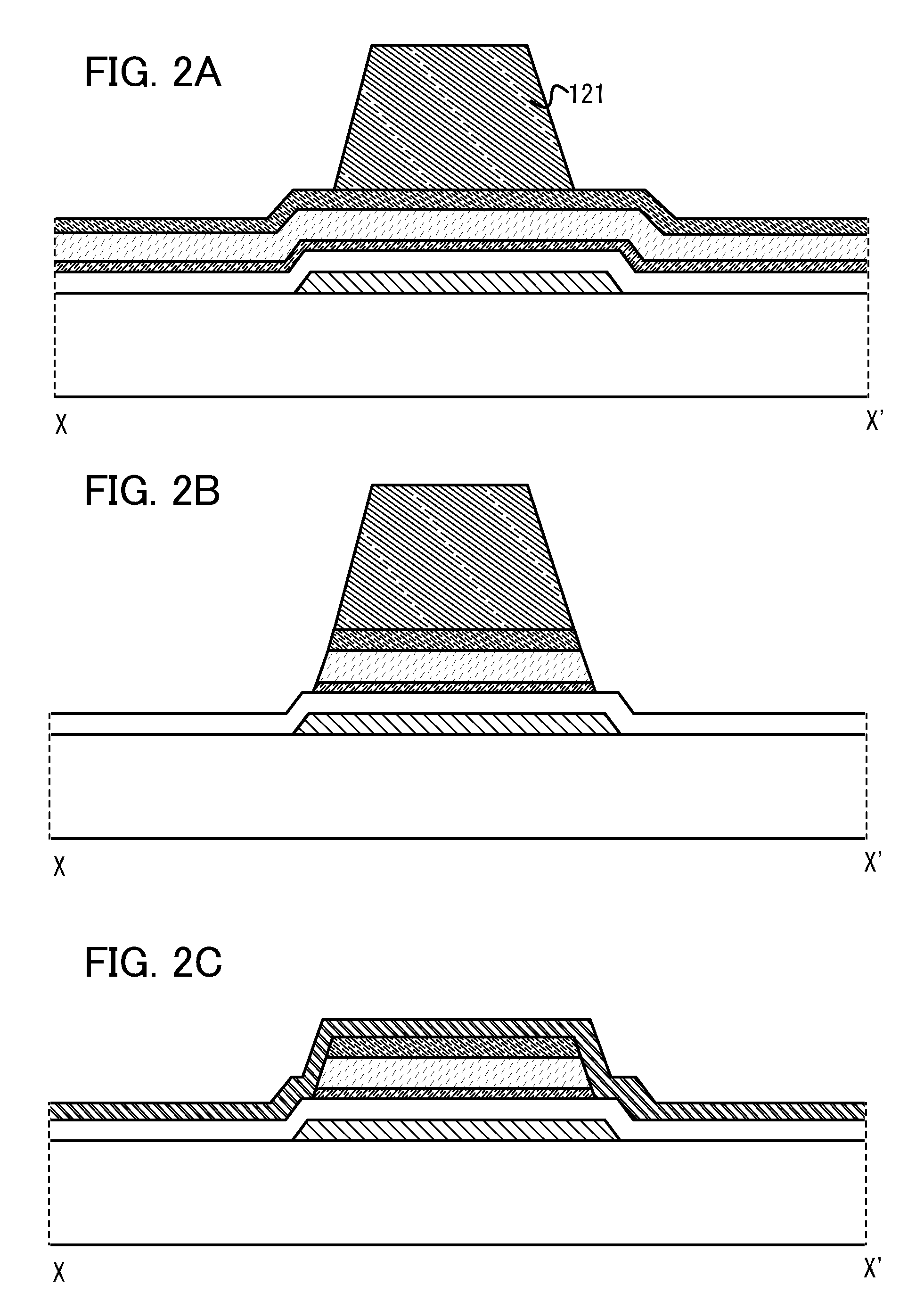
[0248]First, a stacked body in which the steps up to and including the formation of a conductive layer are completed in a manner similar to the manufacturing method described in Embodiment 1 or the like is obtained. Then, a resist mask 136 having a depression portion at a desired position is formed over the stacked body (see FIG. 11A). The resist mask can be a multi-tone mask. As examples of the multi-tone mask, a grey tone mask or a halftone mask can be given, and a known multi-tone mask may be used.

[0249]Then, a microcrystalline semiconductor layer, an amorphous semiconductor layer, and an impurity semiconductor layer are etched using the resist mask 136. By this etching, the semiconductor laye...


PUM


Abstract

The present invention provides a method for manufacturing a thin film transistor with small leakage current and high switching characteristics. In a method for manufacturing a thin film transistor, a back channel portion is formed in the thin film transistor by conducting etching using a resist mask, the resist mask is removed by removal or the like, and a superficial part of the back channel portion is further etched. Through the steps, components of chemical solution used for the removal, residues of the resist mask, and the like which exist at the superficial part of the back channel portion can be removed and leakage current can be reduced. The further etching step of the back channel portion is preferably conducted by dry etching using an N2 gas or a CF4 gas with bias not applied.

Description

BACKGROUND OF THE INVENTION[0001]1. Field of the Invention[0002]The present invention relates to a method for manufacturing a thin film transistor. Further, the present invention relates to a method for manufacturing a semiconductor device having the thin film transistor. As an example of the semiconductor device, a display device is given, in particular. As an example of the display device, a liquid crystal display device and an EL display device are given.[0003]2. Description of the Related Art[0004]In recent years, thin film transistors formed using a semiconductor thin film (having a thickness of about several nanometers to several hundreds of nanometers) formed over a substrate having an insulating surface (e.g., a glass substrate) have been attracting attentions. Thin film transistors are widely used for ICs (integrated circuits) and electronic devices such as electrooptical devices. In particular, thin film transistors are urgently developed as switching elements of image dis...

Claims


Application Information

Patent Timeline
Patent Type & Authority Applications(United States)
IPC IPC(8): H01L33/00H01L21/336
CPCH01L27/1214H01L29/04H01L27/1288H01L29/66765H01L29/78696H01L29/41733H01L27/1255
Inventor SASAGAWA, SHINYAISHIZUKA, AKIHIROKOMORI, SHIGEKI
Owner SEMICON ENERGY LAB CO LTD
Why Eureka
Try Eureka