Thin film transistor substrate

Inactive Publication Date: 2013-05-23
DAI NIPPON PRINTING CO LTD
View PDF22 Cites 34 Cited by
  • Summary
  • Abstract
  • Description
  • Claims
  • Application Information

AI Technical Summary

Benefits of technology

[0049]The present invention offers an effect that a TFT substr

Problems solved by technology

However, when an insulating layer is formed by using such a vapor deposition method, vacuum facilities necessary for vapor deposition may be needed, or complicated processes such as patterning of a resist, etching of inorganic compounds, and peeling of the resist may be needed in order to form patterned insulating layers.
Thus, there is a problem of increasing production cost.
Furthermore, an insulating layer which uses an inorganic compound has a problem that the insulating layer is susceptible to cracking when used in a flexible substrate.
Furthermore, in an insulating layer which uses an inorganic compound, it i

Method used


Image

  • Thin film transistor substrate
  • Thin film transistor substrate
  • Thin film transistor substrate

Examples


Example

Preparation Example 1

[0566]4.0 g (20 mmol) of 4,4′-diaminodiphenyl ether (ODA) and 8.65 g (80 mmol) of para-phenylenediamine (PPD) were introduced into a 500 ml separable flask and were dissolved in 200 g of dehydrated N-methyl-2-pyrrolidone (NMP). Under a nitrogen gas stream, the solution was heated and stirred in an oil bath such that the liquid temperature was monitored with a thermocouple to be increased to 50° C. After it was confirmed that the compounds were completely dissolved, 29.1 g (99 mmol) of 3,3′,4,4′-biphenyltetracarboxylic acid dianhydride (BPDA) was added thereto over 30 minutes in small portions, and after completion of the addition, the mixture was stirred for 5 hours at 50° C. Thereafter, the mixture was cooled to room temperature, and thus a polyimide precursor solution 1 was obtained.

Example

Preparation Example 2

[0567]Polyimide precursor solutions 2 to 17 were synthesized at the mixing ratios indicated in the following Table 1, by the same method as that used in Preparation Example 1, except that the reaction temperature was adjusted, and the amount of NMP was adjusted so that the concentration of the solution would be 17% by weight to 19% by weight.

[0568]As the acid dianhydride, 3,3′,4,4′-biphenyltetracarboxylic acid dianhydride (BPDA) or pyromellitic acid dianhydride (PMDA), p-phenylenebistrimellitic acid monoester acid dianhydride (TAHQ), or p-biphenylenebistrimellitic acid monoester acid dianhydride (BPTME) was used. As the diamine, one kind or two kinds of 4,4′-diaminodiphenyl ether (ODA), para-phenylenediamine (PPD), 1,4-bis(4-aminophenoxy)benzene (4APB), 2,2′-dimethyl-4,4′-diaminobiphenyl (TBHG), and 2,2′-bis(trifluoromethyl)-4,4-diaminobiphenyl (TFMB) were used.

TABLE 1Acid dianhydrideDiamineDiamineAmount ofAmount ofAmount ofReactionadditionadditionadditiontemper...

Example

Preparation Example 3

[0608]The photobase generator 3 was added to the polyimide precursor solution 11 in an amount of 15% by weight of the solids content of the solution, and thus a photosensitive polyimide resin composition 3 was obtained.


PUM

PropertyMeasurementUnit
Temperatureaaaaaaaaaa

Abstract

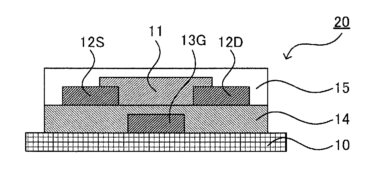
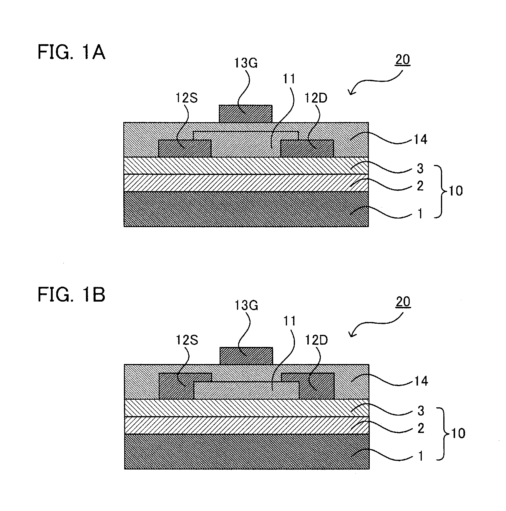
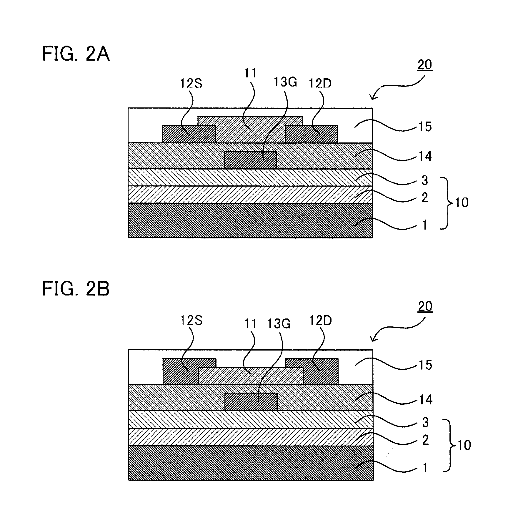
A main object of the present invention is to provide a TFT substrate having excellent switching characteristics. The object is attained by providing a thin film transistor substrate comprising: a substrate, and a thin film transistor having an oxide semiconductor layer that is formed on the substrate and is formed from an oxide semiconductor, and a semiconductor layer-adjoining insulating layer formed to be in contact with the oxide semiconductor layer, wherein at least one semiconductor layer-adjoining insulating layer included in the thin film transistor is a photosensitive polyimide insulating layer formed by using a photosensitive polyimide resin composition.

Description

TECHNICAL FIELD[0001]The present invention relates to a thin film transistor substrate having excellent switching characteristics.BACKGROUND ART[0002]It is a trend of recent years that the range of applications of semiconductor transistors, which are represented by thin film transistors (hereinafter, may be referred to as TFTs), is ever expanding along with the development of display apparatuses. Such a semiconductor transistor has electrodes connected to one another through a semiconductor material, and thereby, the semiconductor transistor accomplishes the function as a switching element.[0003]Regarding the insulating layers such as a gate insulating layer and a passivation layer that are used in TFTs, insulating layers formed by a vapor deposition method using an inorganic compound such as silicon oxide have been put to use (for example, JP 2000-324368 A).[0004]However, when an insulating layer is formed by using such a vapor deposition method, vacuum facilities necessary for vap...

Claims


Application Information

Patent Timeline
IPC IPC(8): H01L21/02H01L29/40
CPCC08L79/08H01L29/78603H01L29/7869H01L21/02118H01L29/408H01L21/02282G03F7/0387C08G73/105C08G73/1067C08G73/1071H01L29/66969G03F7/0045C08G73/1042
Inventor FUKUDA, SHUNJISAKAYORI, KATSUYAARIHARA, KEITA
Owner DAI NIPPON PRINTING CO LTD
Why Eureka
Try Eureka