Oxide for semiconductor layer of thin-film transistor, sputtering target, and thin-film transistor

Inactive Publication Date: 2013-10-17
KOBE STEEL LTD
View PDF3 Cites 24 Cited by
  • Summary
  • Abstract
  • Description
  • Claims
  • Application Information

AI Technical Summary

Benefits of technology

[0028]The oxide for semiconductor layers of the present invention made it possible to provide thin-film transistors, which have excellent switching characteristics and high stress resistance, and in particular, which show a small threshold voltage variation after positive bias stress tests, thereby having excellent TFT characteristics and high stress re

Problems solved by technology

In particular, a shift of the threshold voltage leads to a lowering in the reliability of display devices with TFTs, such as liquid crystal displays or organic EL displays.
The application of positive bias to the gate electrode for a long time causes the accumulation of electrons on the boundary between the gate insulator layer and the semiconductor layer in the TFTs, resulting in a shift of the threshold voltage responsible for a lowering of reliability as described above.
This method improves stress resistance to positive bias, but requires the formation of an insulator layer fr

Method used


Image

  • Oxide for semiconductor layer of thin-film transistor, sputtering target, and thin-film transistor
  • Oxide for semiconductor layer of thin-film transistor, sputtering target, and thin-film transistor
  • Oxide for semiconductor layer of thin-film transistor, sputtering target, and thin-film transistor

Examples


Example

Example 1

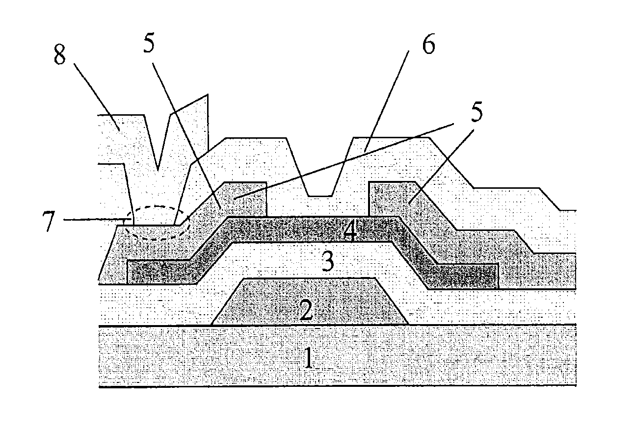
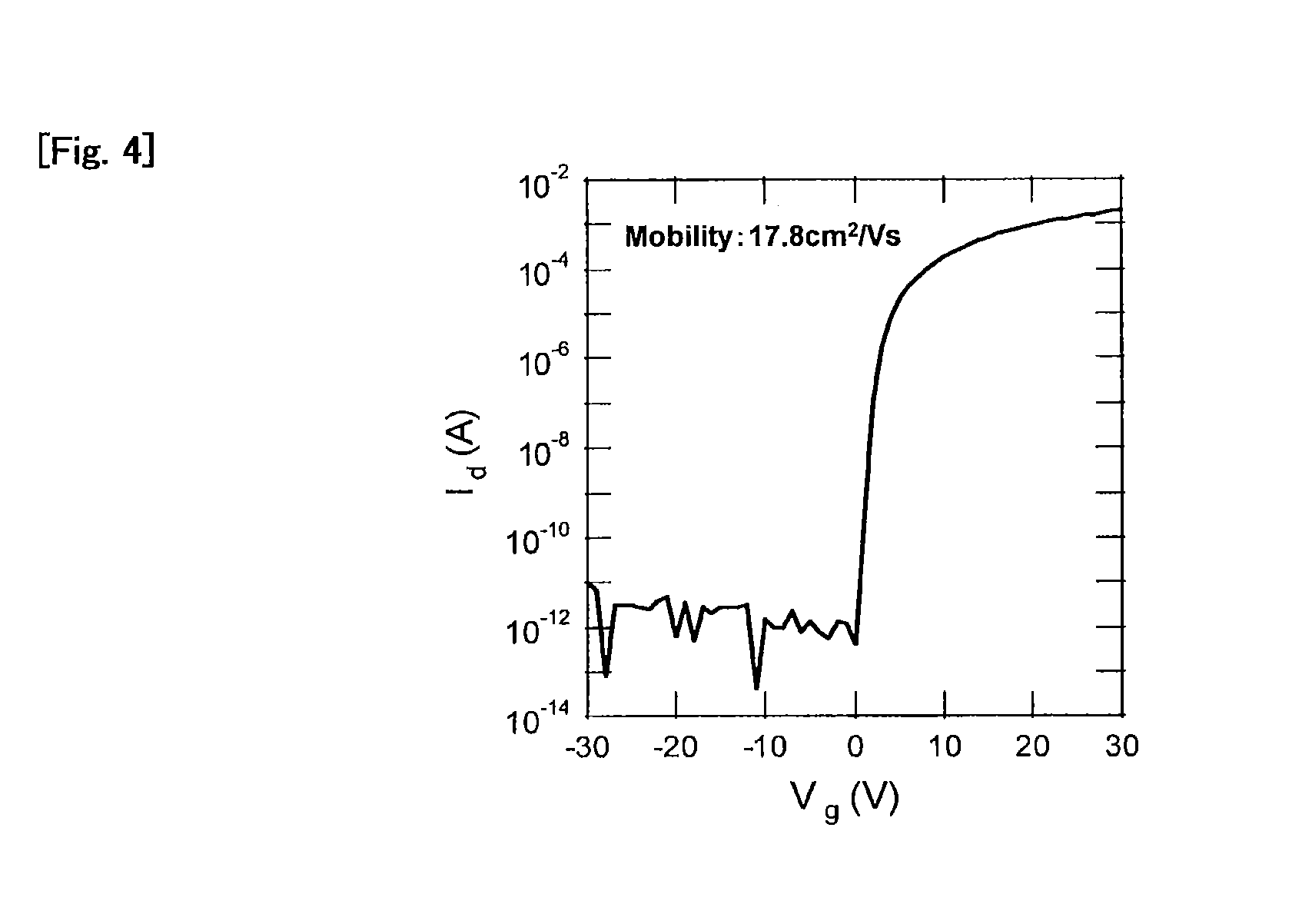
[0075]Based on the method described above, thin-film transistors (TFTs) as shown in FIG. 1 were produced, and the respective characteristics were evaluated.

[0076]First, a Mo thin-film of 100 nm in thickness as a gate electrode and a gate insulator layer of SiO2 (200 nm) were successively formed on a glass substrate (“EAGLE 2000” available from Corning Incorporated, having a diameter 100 mm and a thickness of 0.7 mm). The gate electrode was formed by a DC sputtering method using a pure Mo sputtering target. The sputtering conditions were set as follows: room temperature; film formation power, 3.8 W / cm2; gas pressure, 2 mTorr, and Ar gas flow rate, 20 sccm. The gate insulator layer was formed by a plasma CVD method under the conditions: carrier gas, a mixed gas of SiH4 and N2O; film formation power, 1.27 W / cm3; and film formation temperature, 320° C. The gas pressure during the film formation was set to 133 Pa.

[0077]Then, oxide thin-films of various compositions as shown in T...

Example

Example 2

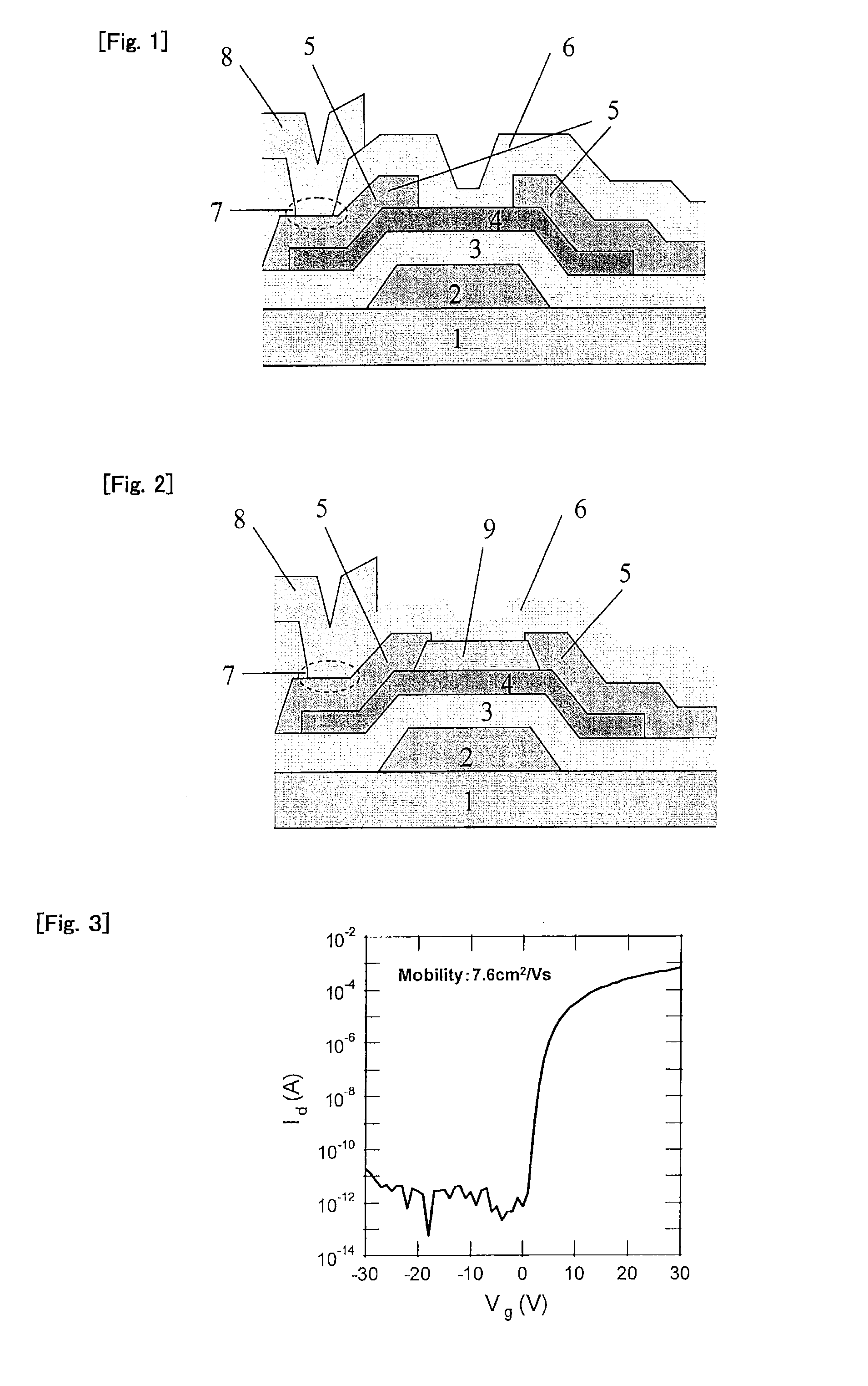
[0129]In this Example, the relationship between the density of each oxide semiconductor layer and the TFT characteristics was examined for the oxides having the compositions shown in Table 2. More specifically, the density of each oxide film (having a thickness of 100 nm) was measured by the method described below, and TFTs were produced and measured for field-effect mobility in the same manner as in Example 1 described above. In Table 2, the oxides of Nos. 1 and 2 in Table 2 have the same composition (In—Zn—Sn—O) as that of as that of No. 2 in Table 1 described above; the oxides of Nos. 3 and 4 in Table 2 have the same composition (In—Zn—Al—O) as that of No. 4 in Table 1; the oxides of Nos. 5 and 6 in Table 2 have the same composition (In—Zn—Ti—O) as that of No. 6 in Table 1; the oxide of No. 7 in Table 2 has the same composition (In—Zn—La—O) as that of No. 8 in Table 1; the oxide of No. 8 in Table 2 has the same composition (In—Zn—Mg—O) as that of No. 9 in Table 1; and th...


PUM

PropertyMeasurementUnit
Densityaaaaaaaaaa
Densityaaaaaaaaaa
Densityaaaaaaaaaa

Abstract

The oxides for semiconductor layers of thin-film transistors according to the present invention include: In; Zn; and at least one element (X group element) selected from the group consisting of Al, Si, Ta, Ti, La, Mg and Nb. The present invention makes it possible to provide oxides for semiconductor layers of thin-film transistors, in which connection thin-film transistors with In—Zn—O oxide semiconductors not containing Ga have favorable switching characteristics and high stress resistance, and in particular, show a small variation of the threshold voltage before and after positive bias stress tests, thereby having high stability.

Description

TECHNICAL FIELD[0001]The present invention relates to an oxide for semiconductor layers of thin-film transistors to be used in display devices such as liquid crystal displays and organic EL displays; a sputtering target for forming the oxide; and a thin-film transistor with the oxide.BACKGROUND ART[0002]As compared with widely used amorphous silicon (a-Si), amorphous (non-crystalline) oxide semiconductors have high carrier mobility (also called as field-effect mobility, which may hereinafter be referred to simply as “mobility”), high optical band gaps, and film formability at low temperatures, and therefore, have highly been expected to be applied for next generation displays, which are required to have large sizes, high resolution, and high-speed drives; resin substrates having low heat resistance; and others.[0003]In the oxide semiconductors, amorphous oxide semiconductors consisting of indium, gallium, zinc and oxygen (In—Ga—Zn—O, which may hereinafter be referred to as “IGZO”) h...

Claims


Application Information

Patent Timeline
IPC IPC(8): H01L27/01
CPCH01L27/016C23C14/086C23C14/3414H01L21/02554H01L21/02565H01L21/02631H01L29/7869H01L27/1225H10K59/1213
Inventor MORITA, SHINYAMIKI, AYAYASUNO, SATOSHIKUGIMIYA, TOSHIHIROKISHI, TOMOYA
Owner KOBE STEEL LTD
Why Eureka
Try Eureka