Semiconductor device and manufacturing method thereof

Active Publication Date: 2013-07-25
SEMICON ENERGY LAB CO LTD
4 Cites 62 Cited by

AI-Extracted Technical Summary

Problems solved by technology

However, as transistors are miniaturized, deterioration in electric characteristics of the transistors, such as lowering in the threshold voltage, an increase of variation in the threshold voltages, and an increase in the amount of off-state current, is likely to Occur.
In addition, as transistors are miniaturized, the transistors are likely to be damaged due to dry etching or affected by diffusion of an impurity element into a semiconductor layer.
As a result, a yield or reliability is l...

Method used

[0170]In other words, the channel formation region, the source region, the drain region, the offset region 506a, and the offset region 506b are formed in a self-aligned manner. By providing the offset regions, parasitic capacitance generated between the channel formation region and the source electrode 505a can be reduced. Further, parasitic capacitance generated between the channel formation region and the drain electrode 505b can be reduced.
[0171]Since the channel formation region is formed in a self-aligned manner, miniaturization of the transistor can be easily achieved, the transistor has excellent on-state characteristics (for example, on-state current and field-effect mobility) and can operate at high speed.
[0179]For example, high mobility can be obtained relatively easily in the case of using an In—Sn—Zn oxide. However, mobility can be increased by reducing the defect density in a bulk also in the case of using an In—Ga—Zn-based oxide.
[0189]With use of the CAAC-OS in a transistor, a change in electric characteristics of the transistor due to irradiation with visible light or ultraviolet light is small. Thus, the transistor has high reliability.
[0191]In an oxide semiconductor having a crystal portion such as the CAAC-OS, defects in the bulk can be further reduced and when the surface flatness of the oxide semiconductor is improved, mobility higher than that of an oxide semiconductor in an amorphous state can be obtained. In order to improve the surface flatness, the oxide semiconductor is preferably formed over a flat surface. Specifically, the oxide semiconductor may be formed over a surface with an arithmetic average surface roughness (Ra) of less than or equal to 1 nm, preferably less than or equal to 0.3 nm, further preferably less than or equal to 0.1 nm.
[0201]The insulating layer 536 may be either a single layer or a stacked layer. In this embodiment, a stack of the insulating layer 536a and the insulating layer 536b is used as the insulating layer 536. The insulating layer 536a formed over the substrate 500 is preferably formed using a material having a barrier property against oxygen and an impurity such as hydrogen, moisture, hydride, or hydroxide, for example, silicon nitride or aluminum oxide. Since the insulating layer 536b formed over the insulating layer 536a is in contact with the oxide semiconductor layer 503, the insulating layer 536b preferably contains oxygen in a proportion higher than that in the stoichiometric composition in the layer (bulk). For example, in the case where the insulating layer 536b is formed using silicon oxide, the composition formula is SiO2+α (α>0). By using the insulating layer 536b as described, oxygen can be supplied to the oxide semiconductor layer 503, leading to favorable characteristics. By supply of oxygen to the oxide semiconductor layer 503, oxygen vacancies in the oxide semiconductor layer 503 can be filled.
[0222]The substrate is held in a deposition chamber kept under reduced pressure. Then, a sputtering gas from which hydrogen and moisture are removed is introduced while residual moisture in the deposition chamber is removed, and the oxide semiconductor layer 503 is deposited over the substrate 500 using the above target. In order to remove moisture remaining in the deposition chamber, an entrapment vacuum pump such as a cryopump, an ion pump, or a titanium sublimation pump is preferably used. As an evacuation unit, a turbo molecular pump to which a cold trap is added may be used. In the deposition chamber which is evacuated with a cryopump, a hydrogen atom, a compound containing a hydrogen atom such as water (H2O) (more preferably, also a compound containing a carbon atom), and the like are removed, whereby the impurity concentration in the oxide semiconductor layer 503 formed in the deposition chamber can be reduced.
[0232]By the introduction (supply) of oxygen to the dehydrated or dehydrogenated oxide semiconductor layer 503, oxygen vacancies in the oxide semiconductor, which are generated in a step of removing an impurity for dehydration or dehydrogenation, can be reduced and the oxide semiconductor layer 503 can be an i-type (intrinsic) oxide semiconductor layer. Variation in electric characteristics of a transistor including the electrically i-type (intrinsic) oxide semiconductor layer 503 is suppressed, and the transistor is electrically stable.
[0237]Note that an oxide semiconductor which is highly purified (purified OS) by reduction of impurities such as moisture or hydrogen which serves as an electron donor (donor) can be made to be an i-type (intrinsic) oxide semiconductor or an oxide semiconductor extremely close to an i-type oxide semiconductor (a substantially i-type oxide semiconductor) by supplying oxygen to the oxide semiconductor to reduce oxygen vacancies in the oxide semiconductor. A transistor including the i-type or substantially i-type oxide semiconductor in a semiconductor layer in which a channel is formed has characteristics of very small off-state current.
[0243]Note that in order to improve coverage with the gate insulating layer 542, the surface of the oxide semiconductor layer 503 may also be subjected to the above-described planarization treatment. In particular, in the case where a thin insulating layer is used as the gate insulating layer 542, it is preferable that the oxide semiconductor layer 503 have improved surface flatness.
[0250]It is preferable that the gate insulating layer 542 include oxygen in a portion which is in contact with the oxide semiconductor layer 503. In this embodiment, the gate insulating layer 542a which is in contact with the oxide semiconductor layer 503 preferably contains oxygen in a proportion higher than that in the stoichiometric composition in the layer (bulk). For example, in the case where silicon oxide is used for the gate insulating layer 542a, the composition formula is SiO2+α (α>0). In this embodiment, silicon oxide of SiO2+α (α>0) is used for the gate insulating layer 542a. By using the silicon oxide for the gate insulating layer 542, oxygen can be supplied to the oxide semiconductor layer 503, leading to good characteristics. Further, the gate insulating layer 542a is preferably formed in consideration of the size of a transistor and the step coverage with the gate insulating layer 542a.
[0254]By introduction of oxygen, a bond between hydrogen and a constituent element of the gate insulating layer 542 or a bond between the constituent element and a hydroxyl group is cut, and the hydrogen or the hydroxyl group reacts with the oxygen, so that water is produced. Accordingly, heat treatment performed after introduction of oxygen facilitates elimination of the hydrogen or the hydroxyl group, which is an impurity, as water. In other words, the impurity concentration in the gate insulating layer 542 can be further reduced by heat treatment. Therefore, heat treatment may be performed after introduction of oxygen into the gate insulating layer 542. After that, oxygen may be further introduced into the gate insulating layer 542 so that the gate insulating layer 542 is in an oxygen-excess state. The introduction of oxygen into the gate insulating layer 542 and the heat treatment may be performed alternately a plurality of times. The introduction of oxygen and the heat treatment may be performed at the same time. Note that the introduction of oxygen may be performed on either one or both of the gate insulating layer 542a and the gate insulating layer 542b.
[0258]A resist mask for forming the gate electrode 501 and the insulating layer 513 by selectively etching part of the conductive layer 504 and part of the insulating layer 508 may be formed by a printing method or an inkjet method. Formation of the resist mask by an inkjet method needs no photomask; thus, manufacturing cost can be reduced.
[0280]The treatment for removing impurities enables a highly reliable transistor having stable electric characteristics. Note that the treatment for removing impurities may also be performed after the gate insulating layer 502 is formed.
[0286]By the introduction of oxygen, a bond between a constituent element of the insulating layer and hydrogen or a bond between the constituent element and a hydroxyl group is cut, and the hydrogen or the hydroxyl group reacts with oxygen to produce water; this leads to easy elimination of hydrogen or a hydroxyl group that is an impurity, in the form of water by heat treatment performed after the introduction of oxygen. In other words, the concentration of impurities in the insulating layer can be further reduced. Therefore, heat treatment may be performed after the introduction of oxygen into the insulating layer, and then oxygen may be further introduced into the insulating layer to make the insulating layer in an oxygen-excess state. The introduction of oxygen into the insulating layer and the heat treatment may be performed alternately a plurality of times. The heat treatment and the introduction of oxygen may be performed at the same time.
[0289]Although the chemical mechanical polishing method is employed for removing the insulating layer 546, the insulating layer 547, and the conductive layer 545 in this embodiment, a different cutting (grinding or polishing) method may be employed. Further, in addition to the cutting (grinding or polishing) method such as a chemical mechanical polishing method, etching (dry etching or wet etching), plasma treatment, or the like may be employed in combination for the step of removing the conductive layer 545 over the gate electrode 501. For example, after the removing step by a chemical mechanical polishing method, a dry etching method or plasma treatment (e.g., reverse sputtering method) may be performed in order to improve the planarity of a surface to be processed. In the case where a cutting (grinding or polishing) method is combined with etching, plasma treatment, or the like, the order of the steps is not limited and may be set as appropriate in accordance with the material, thickness, and surface unevenness of the insulating layer 546, the insulating layer 547, and the conductive layer 545.
[0293]The source electrode 505a and the drain electrode 505b are in contact with the sidewall insulating layer 512 and an exposed portion of a top surface of the oxide semiconductor layer 503. Accordingly, the distance between the gate electrode 501 and a region (a source region or a drain region) in which the oxide semiconductor layer 503 is in contact with the source electrode 505a or the drain electrode 505b corresponds to a width of the sidewall insulating layer 512 in the channel length direction; thus, further miniaturization can be achieved and variation in the manufacturing process can be suppressed.
[0294]Accordingly, the distance between the gate electrode 501 and the region (the source region or the drain region) in which the oxide semiconductor layer 503 is in contact with the source electrode 505a or the drain electrode 505b can be made short, so that the resistance between the gate electrode 501 and the region (the source region or the drain region) in which the oxide semiconductor layer 503 is in contact with the source electrode 505a or the drain electrode 505b is reduced; thus, the on-state characteristics of the transistor 540a can be improved.
[0295]Further, precise processing can be performed accurately because etching with use of a resist mask is not performed when the conductive layer 545 over the gate electrode 501 is removed in a formation step of the source electrode 505a and the drain electrode 505b. Consequently, in a process for manufacturing the semiconductor device, the transistor 540a having a miniaturized structure with less variation in shape or characteristics can be manufactured with high yield.
[0304]The aluminum oxide layers which can be used as the insulating layers 507 and 510 over the oxide semiconductor layer 503 have a high shielding effect (blocking effect) of preventing penetration of both oxygen and impurities such as hydrogen or moisture.
[0309]In addition, a planarization insulating layer may be formed over the transistor in order to reduce surface unevenness due to the transistor. As the planarization insulating layer, an organic material such as polyimide, an acrylic resin, or a benzocyclobutene-based resin can be used. Other than such organic materials, it is also possible to use a low-dielectric constant material (a low-k material) or the like. Note that the planarization insulating layer may be formed by stacking a plurality of insulating layers formed using any of these materials.
[0317]According to this embodiment, a semiconductor device can be manufactured by a smaller number of photolithography processes than the conventional one because a photolithography process for forming an island-shaped semiconductor layer can be omitted. Therefore, a semiconductor device can be manufactured at low cost with high productivity.
[0322]An oxide semiconductor containing In and Ga at a proportion satisfying In>Ga is used on a channel side, and an oxide semiconductor containing In and Ga at a proportion satisfying In≦Ga is used on a back channel side, so that field-effect mobility and reliability of a transistor can be further improved.
[0329]Oxygen is introduced each time the oxide semiconductor layer is formed, whereby the effect of reducing oxygen vacancies in the oxide semiconductor can be improved.
[0345]The transistor 362 illustrated in FIG. 5A includes an oxide semiconductor in the channel formation region. Here, the oxide semiconductor layer 344 included in the transistor 362 is preferably formed using an i-type or substantially i-type oxide semiconductor. By using an i-type oxide semiconductor, the transistor 362 which has extremely favorable off-state characteristics can be obtained.
[0346]Since the off-state current of the transistor 362 is small, stored data can be held for a long time owing to such a transistor. In other words, power consumption can be sufficiently reduced because a semiconductor storage device in which refresh operation is unnecessary or the frequency of refresh operation is extremely low can be provided.
[0349]Further, precise processing can be performed accurately because etching treatment with use of a resist mask is not performed in a step of removing the conductive layer over the gate electrode 348 for forming the electrodes 342a and 342b. Consequently, in a process for manufacturing the semiconductor device, a transistor having a miniaturized structure with less variation in shape or characteristics can be manufactured with high yield.
[0356]In FIGS. 5A and 5B, the transistor 360 is provided so as to overlap with at least part of the transistor 362. The source region or the drain region of the transistor 360 is preferably provided so as to overlap with part of the oxide semiconductor layer 344. Further, the transistor 362 and the capacitor 364 are provided so as to overlap with at least part of the transistor 360. For example, the wiring 354 of the capacitor 364 is provided so as to overlap with at least part of the gate electrode 310 of the transistor 360. With such a planar layout, the area occupied by the semiconductor device can be reduced; thus, higher integration can be achieved.
[0365]Further, in the semiconductor device described in this embodiment, high voltage is not needed for writing data and there is no problem of deterioration of elements. For example, unlike a conventional nonvolatile memory, it is not necessary to inject and extract electrons into and from a floating gate, and thus a problem such as deterioration of a gate insulating layer does not occur at all. In other words, the semiconductor device according to one embodiment of the present invention does not have a limit on the number of times of writing which is a problem in a conventional nonvolatile memory, and reliability thereof is drastically improved. Furthermore, data is written depending on the on state and the off state of the transistor, whereby high-speed operation can be easily realized.
[0366]As described above, a miniaturized and highly-integrated semiconductor device having high electric characteristics and a method for manufacturing the semiconductor device can be provided. Further, a semiconductor device can be provided at low cost and high yield because the semiconductor device can be manufactured by a smaller number of photolithography processes than the conventional one.
[0377]As described above, the semiconductor device illustrated in FIG. 7A can hold charge that is accumulated in the capacitor 754 for a long time because the off-state current of the transistor 362 is extremely small. In other words, power consumption can be adequately reduced because refresh operation becomes unnecessary or the frequency of refresh operation can be extremely low. Moreover, stored data can be held for a long time even when power is not supplied.
[0380]In the structure illustrated in FIG. 7B, the peripheral circuit 753 can be provided under the memory cell array 751. Thus, the size of the semiconductor device can be decreased.
[0381]It is preferable that a semiconductor material of the transistor provided in the peripheral circuit 753 be different from that of the transistor 362. For example, silicon, germanium, silicon germanium, silicon carbide, gallium arsenide, or the like can be used, and a single crystal semiconductor is preferably used. Alternatively, an organic semiconductor material or the like may be used. A transistor including such a semiconductor material can operate at sufficiently high speed. Therefore, a variety of circuits (e.g., a logic circuit or a driver circuit) which needs to operate at high speed can be favorably realized by the transistor.
[0397]A semiconductor device having a novel feature can be obtained by being provided with both a peripheral circuit including the transistor including a material other than an oxide semiconductor (in other words, a transistor capable of operating at sufficiently high speed) and a memory circuit including the transistor including an oxide semiconductor (in a broader sense, a transistor whose amount of off-state current is sufficiently small). In addition, with a structure where the peripheral circuit and the memory circuit are stacked, the degree of integration of the semiconductor device can be increased.
[0398]As described above, a miniaturized and highly-integrated semiconductor device having high electric characteristics and a method for manufacturing the semiconductor device can be provided. Further, a semiconductor device can be provided at low cost and high yield because the semiconductor device can be manufactured by a smaller number of photolithography processes than the conventional one.
[0403]The oxide semiconductor layer 103 includes a channel formation region 131 overlapping with the gate electrode 101 with the gate insulating layer 102 provided therebetween, a source region 133a in contact with the source electrode 105a, a drain region 133b in contact with the drain electrode 105b, an offset region 132a provided between the source region 133a and the channel formation region 131, and an offset region 132b provided between the drain region 133b and the channel formation region 131. In other words, the channel formation region 131, the source region 133a, the drain region 133b, the offset region 132a, and the offset region 132b are formed in a self-aligned manner. By providing the offset region 132a, parasitic capacitance generated between the channel formation region 131 and the source electrode 105a can be reduced. Further, by providing the offset region 132b, parasitic capacitance generated between the channel formation region 131 and the drain electrode 105b can be reduced. Note that the length of the channel formation region 131, which is the distance within which carriers flow (also referred to as channel length), is preferably less than 60 nm.
[0404]Since the channel formation region 131 is formed in a self-aligned manner, miniaturization of the transistor can be easily achieved, the transistor has excellent on-state characteristics (for example, on-state current and field-effect mobility) and can operate at high speed.
[0407]As the substrate 100 having an insulating surface, any substrate can be used as long as it has heat resistance high enough to withstand heat treatment performed later. For example, a substrate such as a glass substrate, a ceramic substrate, a quartz substrate, or a sapphire substrate can be used. A flexible substrate may alternatively be used as the substrate 100 having an insulating surface. The first base insulating layer 137 is formed over the substrate 100 in order to prevent an element contained in the substrate 100 from entering the oxide semiconductor layer 103 to be formed later.
[0414]The oxide semiconductor layer is formed in such a manner that a sputtering gas from which hydrogen and moisture are removed is introduced into a deposition chamber while moisture remaining in the deposition chamber is removed, whereby the concentration of hydrogen in the oxide semiconductor layer can be reduced. In order to remove moisture remaining in the deposition chamber, an entrapment vacuum pump such as a cryopump, an ion pump, or a titanium sublimation pump is preferably used. As an evacuation unit, a turbo molecular pump to which a cold trap is added may be used. In the deposition chamber which is evacuated with a cryopump, a hydrogen atom, a compound containing a hydrogen atom such as water (H2O) (more preferably, also a compound containing a carbon atom), and the like are removed, whereby the impurity concentration in the oxide semiconductor layer 103 formed in the deposition chamber can be reduced.
[0416]In order to reduce the impurity concentration in the oxide semiconductor layer 103, it is also effective to form the oxide semiconductor layer 103 while the substrate 100 is kept at high temperature. The temperature at which the substrate 100 is heated may be higher than or equal to 150° C. and lower than or equal to 450° C.; the substrate temperature is preferably higher than or equal to 200° C. and lower than or equal to 350° C. A crystalline oxide semiconductor layer can be formed by heating the substrate at a high temperature in the formation.
[0427]In addition, after the oxide semiconductor layer 103 is heated in the heat treatment, a high-purity oxygen gas, a high-purity dinitrogen monoxide gas, or ultra dry air (the moisture amount is less than or equal to 20 ppm (−55° C. by conversion into a dew point), preferably less than or equal to 1 ppm, further preferably less than or equal to 10 ppb, in the measurement with use of a dew point meter of a cavity ring down laser spectroscopy (CRDS) system) may be introduced into the same furnace while the heating temperature is maintained or slow cooling is performed to lower the temperature from the heating temperature. It is preferable that water, hydrogen, or the like be not contained in the oxygen gas or the dinitrogen monoxide gas. Alternatively, the purity of the oxygen gas or the dinitrogen monoxide gas which is introduced into the heat treatment apparatus is preferably 6N or higher, further preferably 7N or higher (i.e., the impurity concentration in the oxygen gas or the dinitrogen monoxide gas is preferably 1 ppm or lower, further preferably 0.1 ppm or lower). The oxygen gas or the dinitrogen monoxide gas acts to supply oxygen that is a main component of the oxide semiconductor and that has been reduced by removing an impurity for the dehydration or dehydrogenation, so that the oxide semiconductor layer 103 can have high purity and be an i-type (intrinsic) semiconductor.
[0429]Introduction (supply) of oxygen to the dehydrated or dehydrogenated oxide semiconductor layer 103 enables the oxide semiconductor layer 103 to be highly purified and to be i-type (intrinsic). Variation in electric characteristics of a transistor including the highly purified and i-type (intrinsic) oxide semiconductor layer 103 is suppressed, and the transistor is electrically stable.
[0435]Next, the gate insulating layer 102 covering the oxide semiconductor layer 103 is formed without the oxide semiconductor layer 103 being processed into a predetermined shape. The oxide semiconductor layer 103 is left as formed over the substrate 100 with the first base insulating layer 137 and the second base insulating layer 136 provided therebetween, without being processed into a predetermined shape; thus, the oxide semiconductor layer 103 does not have a side surface of the semiconductor layer where a parasitic channel, which might be a transmission path of leakage current, is easily generated. Without a side surface of the semiconductor layer where a parasitic channel, which might be a transmission path of leakage current, is easily generated, a side surface of the oxide semiconductor layer 103 and a region in the vicinity of the side surface is prevented from becoming a low-resistance region. This can suppress formation of a parasitic channel in a transistor including the oxide semiconductor layer 103. Further, the suppression of formation of a parasitic channel can suppress change in the electric characteristics of the transistor.
[0437]Since the oxide semiconductor layer 103 is not processed into a predetermined shape, there is no need to form a mask for such processing. Therefore, the number of masks can be reduced in the manufacturing process of the transistor of this embodiment.
[0439]The gate insulating layer 102 can be formed using silicon oxide, gallium oxide, aluminum oxide, silicon nitride, silicon oxynitride, aluminum oxynitride, silicon nitride oxide, or the like. The first gate insulating layer 102a, which is in contact with the oxide semiconductor layer 103, of the gate insulating layer 102 preferably contains oxygen. In particular, the first gate insulating layer 102a preferably includes an oxygen-excess region in a region in contact with the oxide semiconductor layer 103, as in the case of the second base insulating layer 136. In particular, it is preferable that the oxygen content of the first gate insulating layer 102a in (a bulk of) the film be in excess of that in the stoichiometric composition. For example, in the case where silicon oxide is used for the first gate insulating layer 102a, the composition formula thereof is preferably SiO2+α (α>0). In this embodiment, silicon oxide of SiO2+α (α>0) is used for the first gate insulating layer 102a. By using the silicon oxide for the first gate insulating layer 102a, oxygen can be supplied to the oxide semiconductor layer 103, leading to good characteristics. Further, the first gate insulating layer 102a is preferably formed in consideration of the size of a transistor to be formed and the step coverage with the first gate insulating layer 102a.
[0440]The second gate insulating layer 102b, which is in contact with the gate electrode 101, of the gate insulating layer 102 has a function of preventing entry of an element contained in the gate electrode 101 to the oxide semiconductor layer 103, and also functions as a blocking layer for suppressing release of oxygen from the oxide semiconductor layer 103.
[0441]The gate insulating layer 102 can be formed using a high-k material such as hafnium oxide, yttrium oxide, hafnium silicate (HfSixOy (x>0, y>0)), hafnium silicate to which nitrogen is added (HfSiOxNy (x>0, y>0)), hafnium aluminate (HfAlxOy (x>0, y>0)), or lanthanum oxide, whereby gate leakage current can be reduced. Furthermore, each of the first gate insulating layer 102a and the second gate insulating layer 102b may have either a single-layer structure or a stacked-layer structure.
[0453]As in the case of formation of the oxide semiconductor layer 103, an entrapment vacuum pump (e.g., a cryopump) is preferably used in order to remove moisture remaining in a deposition chamber of the first insulating layer 106. The first insulating layer 106 is formed in the deposition chamber evacuated using a cryopump, whereby the concentration of impurities in the first insulating layer 106 can be reduced. As an evacuation unit for removing moisture remaining in the deposition chamber of the first insulating layer 106, a turbo molecular pump provided with a cold trap may be used.
[0455]Next, the second insulating layer 107 is formed over the first insulating layer 106 (see FIGS. 11E and 11F). The second insulating layer 107 preferably functions as a planarization insulating layer for suppressing surface unevenness due to the transistor. For the second insulating layer 107, a material appropriately selected from the above-mentioned materials for the first insulating layer 106 can be used. Besides those materials, an organic material such as polyimide, an acrylic resin, or a benzocyclobutene-based resin can be used for the second insulating layer 107. Other than such organic materials, it is also possible to use a low-dielectric constant material (a low-k material) or the like. Note that the planarization insulating layer may be formed by stacking a plurality of insulating layers formed using any of these materials. It is also possible to employ a structure in which the first insulating layer 106 is provided but the second insulating layer 107 is not provided.
[0466]Further, according to this embodiment, a transistor with favorable electric characteristics can be obtained by suppressing formation of a parasitic channel.
[0467]According to one embodiment of the disclosed invention, the number of photolithography processes used for manufacturing a transistor can be reduced to less than the conventional one, so that productivity of transistors can be improved.
[0472]The oxide semiconductor layer 103 includes the channel formation region 131 overlapping with the gate electrode 101 with the gate insulating layer 102 provided therebetween, the source region 133a in contact with the source electrode 115a, the drain region 133b in contact with the drain electrode 115b, the offset region 132a provided between...

Benefits of technology

[0092]According to one embodiment of the present invention, since a semiconductor layer is not processed into an island shape, a side surface of the semiconductor layer, which might be a transmission path of leakage current, is not formed. Therefore, a miniaturized transistor with less variation and favorable electric characteristics can be provided with high yield. Further, it is possible to provide a highly reliable transistor.
[0093]According to one embodiment of the present invention, a transistor can be formed by a smaller number of photolithography processes than the conventional one; thus, productivity of the transistor can be increased.
[0094]Further, also in a semiconductor device including the transistor, high performance, high reliability, and high productivity can be achieved.
[0095]In one embodiment of the present invention, a source electrode and a drain electrode are formed by etching a conductive layer in a state where a mask formed using electron beam exposure is provided over the conductive layer. Here, formation of a mask using electron beam exposure enables minute processing of the mask. Thus, it i...

Abstract

A photolithography process for forming an island-shaped semiconductor layer is omitted, and a transistor is formed by at least two photolithography processes: a photolithography process for forming a gate electrode (including a wiring or the like formed from the same layer as the gate electrode) and a photolithography process for forming a source electrode and a drain electrode (including a wiring or the like formed from the same layer as the source electrode and the drain electrode). By using electron beam exposure, a transistor in which a distance between the source electrode and the drain electrode (channel length) is short can be formed. For example, a transistor whose channel length is less than 50 nm can be obtained.

Application Domain

Technology Topic

Image

  • Semiconductor device and manufacturing method thereof
  • Semiconductor device and manufacturing method thereof
  • Semiconductor device and manufacturing method thereof

Examples

  • Experimental program(12)

Example

Embodiment 1
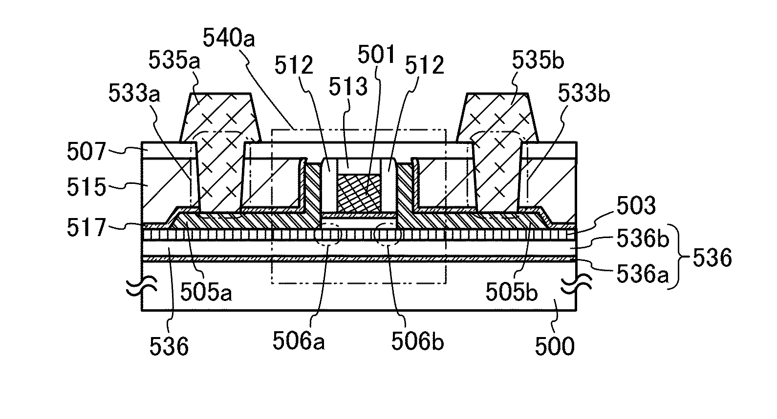
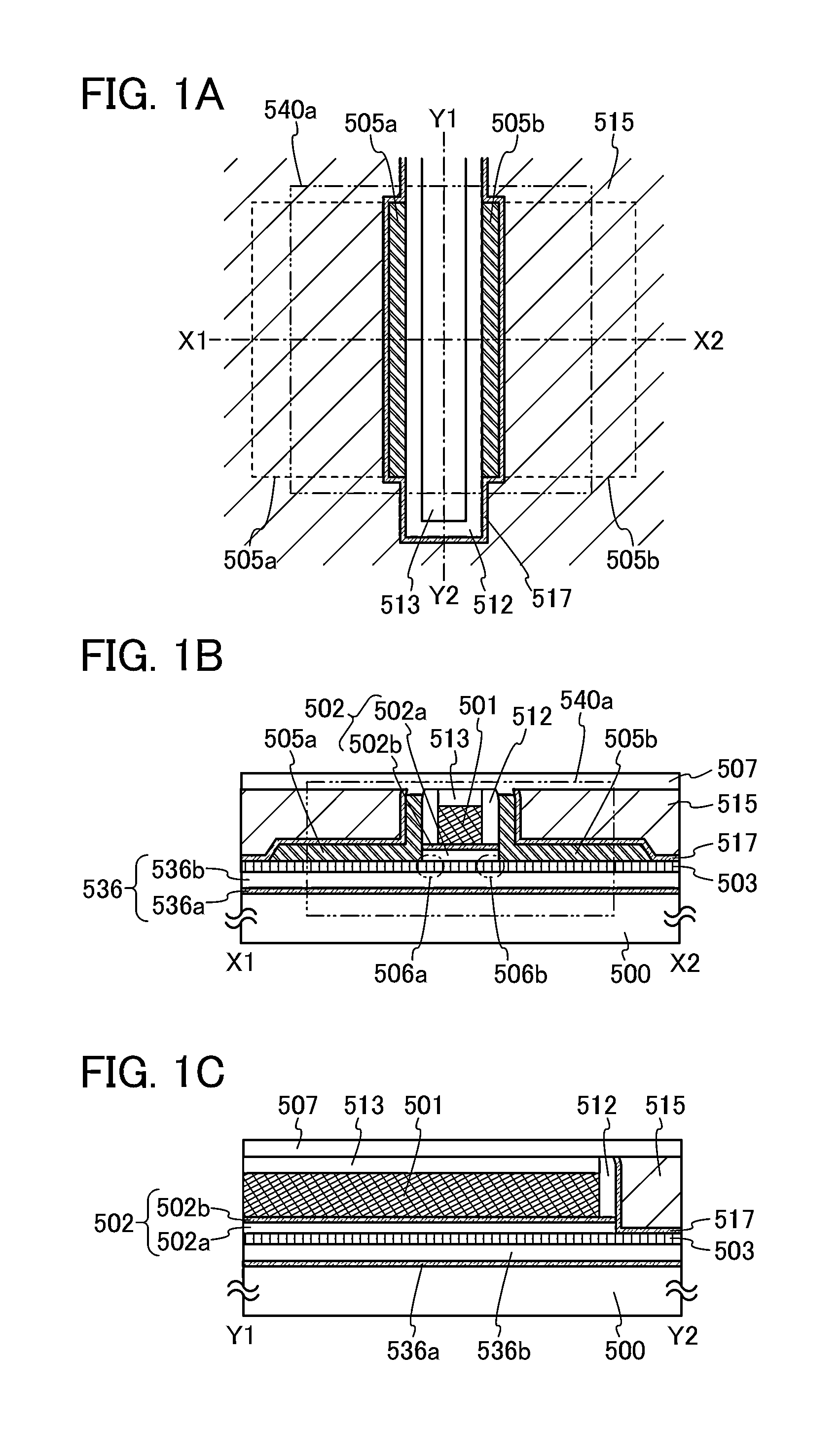
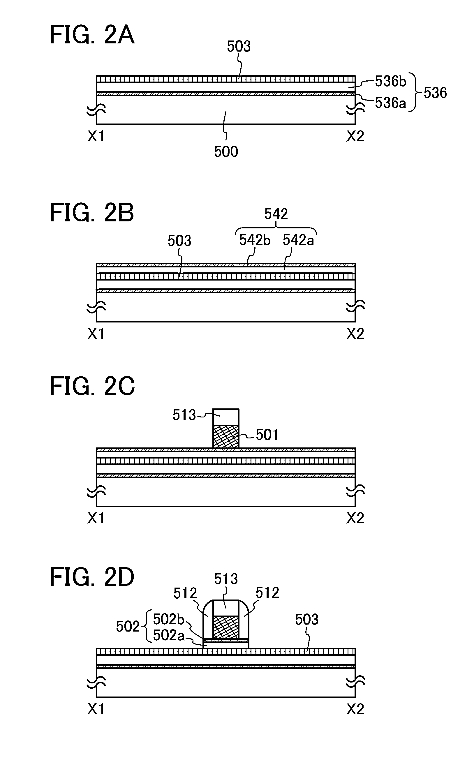
[0162]In this embodiment, one embodiment of a semiconductor device and a method for manufacturing the semiconductor device will be described with reference to FIGS. 1A to 1C. In this embodiment, a transistor including an oxide semiconductor layer is shown as an example of the semiconductor device.
[0163]The transistor may have a single-gate structure in which one channel formation region is formed, a double-gate structure in which two channel formation regions are formed, or a triple-gate structure in which three channel formation regions are formed. Alternatively, the transistor may have a dual gate structure including two gate electrodes positioned over and below a channel region with a gate insulating layer provided therebetween.
[0164]A transistor 540a illustrated in FIGS. 1A to 1C is an example of a top-gate transistor. FIG. 1A is a top view, FIG. 1B is a cross-sectional view along dashed line X1-X2 in FIG. 1A, and FIG. 1C is a cross-sectional view along dashed line Y1-Y2 in FIG. 1A.
[0165]As illustrated in FIG. 1B, which is a cross-sectional view in the channel length direction, and FIG. 1C, which is a cross-sectional view in the channel width direction, a semiconductor device including the transistor 540a includes, over a substrate 500 having an insulating surface over which an insulating layer 536 is provided, an oxide semiconductor layer 503, a source electrode 505a, a drain electrode 505b, a gate insulating layer 502, a gate electrode 501, a sidewall insulating layer 512 provided on a side surface of the gate electrode 501, an insulating layer 513 over the gate electrode 501, an interlayer insulating layer 517 over the source electrode 505a and the drain electrode 505b, an interlayer insulating layer 515 over the insulating layer 517, and an insulating layer 507 covering the transistor 540a. Note that in FIG. 1A, some components are omitted for easy understanding.
[0166]The insulating layer 536 functions as a base layer. An example of the insulating layer 536 in this embodiment is a stack of an insulating layer 536a and an insulating layer 536b. An example of the gate insulating layer 502 in this embodiment is a stack of the gate insulating layer 502a and the gate insulating layer 502b. For each of the insulating layer 536a, the gate insulating layer 502b, and the interlayer insulating layer 517, a material having a barrier property against oxygen or an impurity such as hydrogen, moisture, hydride, or hydroxide is preferably used. By applying a material having a barrier property to the above insulating layers, entry of impurities from the outside can be prevented and release of oxygen from the oxide semiconductor layer 503, the insulating layer 536b, and the gate insulating layer 502a can be prevented.
[0167]The interlayer insulating layer 515 is provided for planarizing unevenness due to the transistor 540a. The height of a top surface of the interlayer insulating layer 515 (here, the “height of a top surface of the interlayer insulating layer 515” means a perpendicular distance from a surface of the substrate 500 to a top surface of the interlayer insulating layer 515) is substantially the same as that of each top surface of the sidewall insulating layer 512 and the insulating layer 513. Further, the height of each top surface of the source electrode 505a and the drain electrode 505b is lower than that of each top surface of the interlayer insulating layer 515, the sidewall insulating layer 512, and the insulating layer 513, and higher than that of a top surface of the gate electrode 501.
[0168]Further, in FIGS. 1A to 1C, the insulating layer 507 is provided in contact with the interlayer insulating layer 515, the interlayer insulating layer 517, the source electrode 505a, the drain electrode 505b, the sidewall insulating layer 512, and the insulating layer 513.
[0169]Note that a region of the oxide semiconductor layer 503 which overlaps with the gate electrode 501 is referred to as a channel formation region, a region of the oxide semiconductor layer 503 which is in contact with the source electrode 505a is referred to as a source region, and a region of the oxide semiconductor layer 503 which is in contact with the drain electrode 505b is referred to as a drain region. Further, a region of the oxide semiconductor layer 503 which is between the channel formation region and the source region is referred to as an offset region 506a, and a region of the oxide semiconductor layer 503 which is between the channel formation region and the drain region is referred to as an offset region 506b. The offset region 506a and the offset region 506b are formed in the oxide semiconductor layer 503 to overlap with the sidewall insulating layer 512.
[0170]In other words, the channel formation region, the source region, the drain region, the offset region 506a, and the offset region 506b are formed in a self-aligned manner. By providing the offset regions, parasitic capacitance generated between the channel formation region and the source electrode 505a can be reduced. Further, parasitic capacitance generated between the channel formation region and the drain electrode 505b can be reduced.
[0171]Since the channel formation region is formed in a self-aligned manner, miniaturization of the transistor can be easily achieved, the transistor has excellent on-state characteristics (for example, on-state current and field-effect mobility) and can operate at high speed.
[0172]An oxide semiconductor to be used for the oxide semiconductor layer 503 preferably contains at least indium (In) or zinc (Zn). In particular, In and Zn are preferably contained. In addition, as a stabilizer for reducing the variation in electric characteristics of a transistor using the oxide semiconductor, the oxide semiconductor preferably contains gallium (Ga) in addition to In and Zn. Tin (Sn) is preferably contained as a stabilizer. Hafnium (Hf) is preferably contained as a stabilizer. Aluminum (Al) is preferably contained as a stabilizer. Zirconium (Zr) is preferably contained as a stabilizer.
[0173]As another stabilizer, one or plural kinds of lanthanoid such as lanthanum (La), cerium (Ce), praseodymium (Pr), neodymium (Nd), samarium (Sm), europium (Eu), gadolinium (Gd), terbium (Tb), dysprosium (Dy), holmium (Ho), erbium (Er), thulium (Tm), ytterbium (Yb), or lutetium (Lu) may be contained.
[0174]For example, the following can be used: indium oxide; tin oxide; zinc oxide; a two-component metal oxide such as an In—Zn-based oxide, a Sn—Zn-based oxide, an Al—Zn-based oxide, a Zn—Mg-based oxide, a Sn—Mg-based oxide, an In—Mg-based oxide, or an In—Ga-based oxide; a three-component metal oxide such as an In—Ga—Zn-based oxide (also referred to as IGZO), an In—Al—Zn-based oxide, an In—Sn—Zn-based oxide, a Sn—Ga—Zn-based oxide, an Al—Ga—Zn-based oxide, a Sn—Al—Zn-based oxide, an In—Hf—Zn-based oxide, an In—La—Zn-based oxide, an In—Ce—Zn-based oxide, an In—Pr—Zn-based oxide, an In—Nd—Zn-based oxide, an In—Sm—Zn-based oxide, an In—Eu—Zn-based oxide, an In—Gd—Zn-based oxide, an In—Tb—Zn-based oxide, an In—Dy—Zn-based oxide, an In—Ho—Zn-based oxide, an In—Er—Zn-based oxide, an In—Tm—Zn-based oxide, an In—Yb—Zn-based oxide, or an In—Lu—Zn-based oxide; or a four-component metal oxide such as an In—Sn—Ga—Zn-based oxide, an In—Hf—Ga—Zn-based oxide, an In—Al—Ga—Zn-based oxide, an In—Sn—Al—Zn-based oxide, an In—Sn—Hf—Zn-based oxide, or an In—Hf—Al—Zn-based oxide.
[0175]Note that here, for example, an “In—Ga—Zn-based oxide” means an oxide containing In, Ga, and Zn as its main component and there is no particular limitation on the ratio of In:Ga:Zn. The In—Ga—Zn-based oxide may contain a metal element other than the In, Ga, and Zn.
[0176]Alternatively, a material represented by InMO3(ZnO)m (m>0) may be used as an oxide semiconductor. Note that M represents one or more metal elements selected from Ga, Fe, Mn, and Co. Still alternatively, a material represented by In2SnO5(ZnO)n (n>0) may be used as an oxide semiconductor.
[0177]For example, an In—Ga—Zn-based oxide with an atomic ratio of In:Ga:Zn=1:1:1 (=⅓:⅓:⅓), In:Ga:Zn=2:2:1 (=⅖:⅖:⅕), In:Ga:Zn=3:1:2 (=½:⅙:⅓), or any of oxides whose composition is in the neighborhood of the above compositions can be used. Alternatively, an In—Sn—Zn-based oxide with an atomic ratio of In:Sn:Zn=1:1:1 (=⅓:⅓:⅓), In:Sn:Zn=2:1:3 (=⅓:⅙:½), or In:Sn:Zn=2:1:5 (=¼:⅛:⅝), or any of oxides whose composition is in the neighborhood of the above compositions may be used.
[0178]However, the semiconductor oxide is not limited to the materials given above, but a material with an appropriate composition may be used depending on needed semiconductor characteristics (e.g., mobility, threshold voltage, and variation). In order to obtain the required semiconductor characteristics, it is preferable that the carrier concentration, the impurity concentration, the defect density, the atomic ratio between a metal element and oxygen, the interatomic distance, the density, and the like be set to appropriate values.
[0179]For example, high mobility can be obtained relatively easily in the case of using an In—Sn—Zn oxide. However, mobility can be increased by reducing the defect density in a bulk also in the case of using an In—Ga—Zn-based oxide.
[0180]For example, the case where the composition of an oxide having an atomic ratio where In:Ga:Zn=a:b:c (a+b+c=1) is in the neighborhood of the composition of an oxide having an atomic ratio where In:Ga:Zn=A:B:C (A+B+C=1) means that a, b, and c satisfy the following relation: (a−A)2+(b−B)2+(c−C)2≦r2, and r may be 0.05, for example. The same applies to other oxides.
[0181]As the oxide semiconductor disclosed in this embodiment, a c-axis aligned crystalline oxide semiconductor (CAAC-OS) can be used besides a single crystal oxide semiconductor, a polycrystalline (also referred to as polycrystal) oxide semiconductor, an amorphous oxide semiconductor, and the like.
[0182]There are three methods for obtaining a CAAC-OS layer. The first method is to deposit an oxide semiconductor layer at a deposition temperature higher than or equal to 200° C. and lower than or equal to 450° C., thereby obtaining c-axis alignment substantially perpendicular to a surface. The second method is to deposit a thin oxide semiconductor layer and then subject the layer to a heat treatment performed at a temperature higher than or equal to 200° C. and lower than or equal to 700° C., thereby obtaining c-axis alignment substantially perpendicular to the surface thereof. The third method is to deposit a first thin oxide semiconductor layer, subject the layer to a heat treatment performed at a temperature higher than or equal to 200° C. and lower than or equal to 700° C., and then deposit a second oxide semiconductor layer, thereby obtaining c-axis alignment substantially perpendicular to the surface thereof.
[0183]The CAAC-OS is not completely single crystal or completely amorphous. The CAAC-OS is an oxide semiconductor with a crystal-amorphous mixed phase structure where crystal portions are included in an amorphous phase. Note that in most cases, the crystal part fits inside a cube whose one side is less than 100 nm. From an observation image obtained with a transmission electron microscope (TEM), a boundary between an amorphous portion and a crystal portion in the CAAC-OS is not clear. Further, with the TEM, a grain boundary in the CAAC-OS is not found. Thus, in the CAAC-OS, a reduction in electron mobility, due to the grain boundary, is suppressed.
[0184]In the crystal portion included in the CAAC-OS, the c-axes are aligned in a direction perpendicular to a surface where the CAAC-OS is formed or a surface of the CAAC-OS, triangular or hexagonal atomic arrangement which is seen from the direction perpendicular to the a-b plane is formed, and metal atoms are arranged in a layered manner or metal atoms and oxygen atoms are arranged in a layered manner when seen from the direction perpendicular to the c-axis.
[0185]In other words, in each of the crystal parts included in the CAAC-OS, a c-axis is aligned in a direction parallel to a normal vector of a surface where the CAAC-OS is formed or a normal vector of a surface of the CAAC-OS, triangular or hexagonal atomic arrangement which is seen from the direction perpendicular to the a-b plane is formed, and metal atoms are arranged in a layered manner or metal atoms and oxygen atoms are arranged in a layered manner when seen from the direction perpendicular to the c-axis.
[0186]Note that, among crystal parts, the directions of the a-axis and the b-axis of one crystal portion may be different from those of another crystal portion. In this specification, a simple term “perpendicular” includes a range from 85° to 95°. In addition, a simple term “parallel” includes a range from −5° to 5°.
[0187]In the CAAC-OS, distribution of crystal portions is not necessarily uniform. For example, in the formation process of the CAAC-OS, in the case where crystal growth occurs from a surface side of the oxide semiconductor layer, the proportion of crystal portions in the vicinity of the surface of the oxide semiconductor layer is higher than that in the vicinity of the surface where the oxide semiconductor layer is formed in some cases. Further, when an impurity is added to the CAAC-OS, the crystal portion in a region to which the impurity is added becomes amorphous in some cases.
[0188]Since the c-axes of the crystal portions included in the CAAC-OS are aligned in the direction perpendicular to the surface where the CAAC-OS is formed or a surface of the CAAC-OS, the directions of the c-axes may be different from each other depending on the shape of the CAAC-OS (the cross-sectional shape of the surface where the CAAC-OS is formed or the cross-sectional shape of the surface of the CAAC-OS). The direction of c-axis of the crystal portion is the direction perpendicular to the surface where the CAAC-OS is formed or the surface of the CAAC-OS. The crystal portion is formed by deposition or by performing treatment for crystallization such as heat treatment after deposition.
[0189]With use of the CAAC-OS in a transistor, a change in electric characteristics of the transistor due to irradiation with visible light or ultraviolet light is small. Thus, the transistor has high reliability.
[0190]Note that part of oxygen included in the oxide semiconductor layer may be substituted with nitrogen.
[0191]In an oxide semiconductor having a crystal portion such as the CAAC-OS, defects in the bulk can be further reduced and when the surface flatness of the oxide semiconductor is improved, mobility higher than that of an oxide semiconductor in an amorphous state can be obtained. In order to improve the surface flatness, the oxide semiconductor is preferably formed over a flat surface. Specifically, the oxide semiconductor may be formed over a surface with an arithmetic average surface roughness (Ra) of less than or equal to 1 nm, preferably less than or equal to 0.3 nm, further preferably less than or equal to 0.1 nm.
[0192]Note that, Ra can be expressed as an “average value of the absolute values of deviations from a reference surface to a specific surface” and is defined by the formula (1) below.
[ FORMULA 1 ] Ra = 1 S 0 ∫ y 1 y 2 ∫ x 1 x 2 f ( x , y ) - Z 0 x y
[0193]Here, the specific surface is a surface that is a target of roughness measurement, and is a quadrilateral region specified by four points represented by the coordinates (x1, y1, f(x1, y1)), (x1, y2, f(x1, y2)), (x2, y1, f(x2, y1)), and (x2, y2, f(x2, y2)). Moreover, S0 represents the area of a rectangle which is obtained by projecting the specific surface on the xy plane, and Z0 represents the height of the reference surface (the average height of the specific surface). Ra can be measured using an atomic force microscope (AFM).
[0194]The oxide semiconductor layer has a thickness greater than or equal to 1 nm and less than or equal to 30 nm (preferably greater than or equal to 5 nm and less than or equal to 10 nm) and can be formed by a sputtering method, a molecular beam epitaxy (MBE) method, a CVD method, a pulsed laser deposition method, an atomic layer deposition (ALD) method, or the like as appropriate. The oxide semiconductor layer 503 may be deposited with a sputtering apparatus which performs deposition in the state where top surfaces of a plurality of substrates are substantially perpendicular to a top surface of a sputtering target.
[0195]An example of a method for manufacturing a semiconductor device including the transistor 540a is described with reference to FIGS. 2A to 2D and FIGS. 3A to 3D.
[0196]First, over the substrate 500, the insulating layer 536 is formed.
[0197]There is no particular limitation on a substrate that can be used as the substrate 500 as long as it has heat resistance high enough to withstand heat treatment performed later. For example, a glass substrate of barium borosilicate glass, aluminoborosilicate glass, or the like, a ceramic substrate, a quartz substrate, or a sapphire substrate can be used. A single crystal semiconductor substrate or a polycrystalline semiconductor substrate made of silicon, silicon carbide, or the like; a compound semiconductor substrate made of silicon germanium or the like; an SOI substrate; or the like can be used as the substrate 500, or the substrate provided with a semiconductor element can be used as the substrate 500.
[0198]The semiconductor device may be manufactured using a flexible substrate as the substrate 500. To manufacture a flexible semiconductor device, the transistor 540a including the oxide semiconductor layer 503 may be directly formed over a flexible substrate; or alternatively, the transistor 540a including the oxide semiconductor layer 503 may be formed over a substrate, and then may be separated and transferred to a flexible substrate. Note that in order to separate the transistor 540a from the manufacturing substrate and transfer it to the flexible substrate, a separation layer may be provided between the manufacturing substrate and the transistor 540a including the oxide semiconductor layer 503.
[0199]The insulating layer 536 can be formed using silicon oxide, silicon nitride, silicon oxynitride, silicon nitride oxide, aluminum oxide, aluminum nitride, aluminum oxynitride, aluminum nitride oxide, hafnium oxide, gallium oxide, or a mixed material of any of these materials by a plasma CVD method, a sputtering method, or the like. Note that in this specification, oxynitride contains more oxygen than nitrogen, and nitride oxide contains more nitrogen than oxygen. For example, silicon oxynitride refers to a substance that includes oxygen, nitrogen, and silicon at concentrations ranging from 50 at. % to 70 at. %, 0.5 at. % to 20 at. %, and 25 at. % to 35 at. %, respectively. In addition, the total of the percentages of the constituent elements does not exceed 100 at. %. The oxygen content and the nitrogen content are measured by Rutherford backscattering spectrometry (RBS) or hydrogen forward scattering spectrometry (HFS).
[0200]As the insulating layer 536, a thermal oxidation film may be used. The thermal oxidation film can be formed in the following manner: a substrate is subjected to heat treatment in an oxidation atmosphere, so that a surface of the substrate is oxidized. For example, a single crystal silicon substrate is used as the substrate 500, and heat treatment is performed at 900° C. to 1200° C. in an atmosphere containing oxygen or water vapor for several hours, whereby a thermal oxidation film can be formed on a surface of the substrate 500.
[0201]The insulating layer 536 may be either a single layer or a stacked layer. In this embodiment, a stack of the insulating layer 536a and the insulating layer 536b is used as the insulating layer 536. The insulating layer 536a formed over the substrate 500 is preferably formed using a material having a barrier property against oxygen and an impurity such as hydrogen, moisture, hydride, or hydroxide, for example, silicon nitride or aluminum oxide. Since the insulating layer 536b formed over the insulating layer 536a is in contact with the oxide semiconductor layer 503, the insulating layer 536b preferably contains oxygen in a proportion higher than that in the stoichiometric composition in the layer (bulk). For example, in the case where the insulating layer 536b is formed using silicon oxide, the composition formula is SiO2+α (α>0). By using the insulating layer 536b as described, oxygen can be supplied to the oxide semiconductor layer 503, leading to favorable characteristics. By supply of oxygen to the oxide semiconductor layer 503, oxygen vacancies in the oxide semiconductor layer 503 can be filled.
[0202]In this embodiment, a single crystal silicon substrate is used as the substrate 500, a 50-nm-thick silicon nitride layer is formed over the substrate 500 by a plasma CVD method as the insulating layer 536a, and a 300-nm-thick silicon oxide layer is formed over the insulating layer 536a by a plasma CVD method as the insulating layer 536b (see FIG. 2A).
[0203]The temperature at the time of forming the insulating layer 536 is preferably as high as possible among temperatures that the substrate 500 can withstand. For example, the insulating layer 536 is formed with the substrate 500 heated at a temperature higher than or equal to 350° C. and lower than or equal to 450° C. Note that the temperature at the time of forming the insulating layer 536 is preferably constant. For example, the insulating layer 536 is formed with the substrate 500 heated at 350° C.
[0204]After the formation of the insulating layer 536, heat treatment may be performed under reduced pressure, a nitrogen atmosphere, a rare gas atmosphere, or an ultra-dry atmosphere. The heat treatment can reduce the concentration of hydrogen, moisture, hydride, hydroxide, or the like in the insulating layer 536. It is preferable that the temperature of the heat treatment be as high as possible among temperatures that the substrate 500 can withstand. Specifically, it is preferable that the heat treatment be performed at a temperature higher than or equal to the deposition temperature of the insulating layer 536 and lower than or equal to the strain point of the substrate 500.
[0205]Note that the hydrogen concentration in the insulating layer 536 is preferably lower than 5×10¹⁸ atoms/cm3, further preferably lower than or equal to 1×10¹⁸ atoms/cm3, still further preferably lower than or equal to 5×10¹⁷ atoms/cm3, and further more preferably lower than or equal to 1×10¹⁶ atoms/cm3.
[0206]After formation of the insulating layer 536, oxygen (including at least one of oxygen radicals, oxygen atoms, and oxygen ions) may be introduced into the insulating layer 536 so that the insulating layer 536 includes a region containing oxygen in a proportion higher than that in the stoichiometric composition (includes an oxygen-excess region). For the introduction of oxygen, heat treatment performed in an oxygen atmosphere, an ion implantation method, an ion doping method, a plasma immersion ion implantation method, plasma treatment performed in an atmosphere containing oxygen, or the like can be employed. In the case of performing plasma treatment in an atmosphere containing oxygen, an ashing apparatus can be used, for example.
[0207]By introduction of oxygen, a bond between hydrogen and a constituent element of the insulating layer 536 or a bond between the constituent element and a hydroxyl group is cut, and the hydrogen or the hydroxyl group reacts with the oxygen, so that water is produced. Accordingly, heat treatment performed after introduction of oxygen facilitates elimination of the hydrogen or the hydroxyl group, which is an impurity, as water. Therefore, heat treatment may be performed after introduction of oxygen into the insulating layer 536. After that, oxygen may be further introduced into the insulating layer 536 so that the insulating layer 536 is in an oxygen-excess state. The introduction of oxygen into the insulating layer 536 and the heat treatment may be performed alternately a plurality of times. The introduction of oxygen and the heat treatment may be performed at the same time.
[0208]Next, the oxide semiconductor layer 503 is formed over the insulating layer 536 by a sputtering method (see FIG. 2A).
[0209]In order that hydrogen or water will be not contained in the oxide semiconductor layer 503 as much as possible in the formation step of the oxide semiconductor layer 503, it is preferable to heat the substrate provided with the insulating layer 536 in a preheating chamber of a sputtering apparatus as a pretreatment for deposition of the semiconductor layer 503 so that impurities such as hydrogen and moisture adsorbed to the substrate and the insulating layer 536 are eliminated and evacuated. As an evacuation unit provided in the preheating chamber, a cryopump is preferable.
[0210]Therefore, planarization treatment may be performed on the region of the insulating layer 536 which is to be in contact with the oxide semiconductor layer 503. As the planarization treatment, polishing treatment (e.g., a chemical mechanical polishing method), dry-etching treatment, or plasma treatment can be used, though there is no particular limitation on the planarization treatment.
[0211]As plasma treatment, for example, reverse sputtering in which an argon gas is introduced and plasma is generated can be performed. The reverse sputtering is a method in which voltage is applied to a substrate side with use of an RF power source in an argon atmosphere and plasma is generated in the vicinity of the substrate so that a substrate surface is modified. Note that instead of an argon atmosphere, a nitrogen atmosphere, a helium atmosphere, an oxygen atmosphere, or the like may be used. The reverse sputtering can remove particle substances (also referred to as particles or dust) attached to the top surface of the insulating layer 536.
[0212]As the planarization treatment, polishing treatment, dry etching treatment, or plasma treatment may be performed plural times, or these treatments may be performed in combination. In the case where the treatments are combined, the order of steps is not particularly limited and may be set as appropriate depending on the roughness of the surface of the insulating layer 536.
[0213]Planarization treatment may be performed on a surface of the silicon oxide layer used as the insulating layer 536 by a chemical mechanical polishing method (the polishing conditions: a polyurethane-based polishing cloth, silica-based slurry, a slurry temperature of room temperature, a polishing pressure of 0.001 MPa, a rotation number in polishing (table/spindle) of 60 rpm/56 rpm, and a polishing time of 0.5 minutes) so that the average surface roughness (Ra) of the surface of the silicon oxide layer is preferably approximately 0.15 nm.
[0214]Note that a rare gas (typically argon) atmosphere, an oxygen atmosphere, or a mixed gas of a rare gas and oxygen is used as appropriate as a sputtering gas used for forming the oxide semiconductor layer 503. It is preferable that a high-purity gas from which impurities such as hydrogen, water, a hydroxyl group, and hydride are removed be used as a sputtering gas.
[0215]The oxide semiconductor layer 503 is preferably deposited under a condition such that much oxygen is contained (for example, by a sputtering method in an atmosphere where the proportion of oxygen is 100%) so as to contain much oxygen or oxygen in a supersaturated state (preferably include a region containing oxygen in excess of the stoichiometric composition of the oxide semiconductor in a crystalline state).
[0216]For example, in the case where the oxide semiconductor layer is formed by a sputtering method, the formation is performed preferably under a condition that the proportion of oxygen in the sputtering gas is large, more preferably under a condition that the proportion of oxygen in the sputtering gas is 100%. When film formation is performed under such a condition that the proportion of oxygen in the sputtering gas is high, particularly in a 100% oxygen gas atmosphere, release of Zn from the oxide semiconductor layer can be suppressed even at a formation temperature higher than or equal to 300° C., for example.
[0217]It is preferable that the oxide semiconductor layer 503 be highly purified so as to hardly contain impurities such as copper, aluminum, or chlorine. In a process for manufacturing a transistor, a step which has no risk that such impurities enter the oxide semiconductor layer or adhere to the surface of the oxide semiconductor layer is preferably selected as appropriate. Specifically, the concentration of copper in the oxide semiconductor layer 503 is lower than or equal to 1×10¹⁸ atoms/cm3, preferably lower than or equal to 1×10¹⁷ atoms/cm3. Further, the concentration of aluminum in the oxide semiconductor layer 503 is lower than or equal to 1×10¹⁸ atoms/cm3. Further, the concentration of chlorine in the oxide semiconductor layer 503 is lower than or equal to 2×10¹⁸ atoms/cm3.
[0218]The concentrations of alkali metals such as sodium (Na), lithium (Li), and potassium (K) in the oxide semiconductor layer 503 are preferably as follows. The concentration of Na is 5×10¹⁶ atoms/cm−3 or lower, preferably 1×10¹⁶ atoms/cm−3 or lower, further preferably 1×10¹⁵ atoms/cm−3 or lower. The concentration of Li is 5×10¹⁵ atoms/cm−3 or lower, preferably 1×10¹⁵ atoms/cm−3 or lower. The concentration of K is 5×10¹⁵ atoms/cm−3 or lower, preferably 1×10¹⁵ atoms/cm−3 or lower.
[0219]In this embodiment, as the oxide semiconductor layer 503, a 35-nm-thick In—Ga—Zn-based oxide (IGZO) layer is formed by a sputtering method using a sputtering apparatus including an AC power supply device. As a target for forming the oxide semiconductor layer 503 by a sputtering method, a metal oxide target having an atomic ratio of In:Ga:Zn=3:1:2 is used.
[0220]The relative density (the fill rate) of the metal oxide target is 90% to 100% inclusive, preferably 95% to 99.9% inclusive. By using the metal oxide target with high relative density, a dense oxide semiconductor layer 503 can be formed.
[0221]It is preferable to use a high-purity gas from which impurities such as hydrogen, water, a hydroxyl group, or hydride are removed as a sputtering gas used when the oxide semiconductor layer 503 is deposited.
[0222]The substrate is held in a deposition chamber kept under reduced pressure. Then, a sputtering gas from which hydrogen and moisture are removed is introduced while residual moisture in the deposition chamber is removed, and the oxide semiconductor layer 503 is deposited over the substrate 500 using the above target. In order to remove moisture remaining in the deposition chamber, an entrapment vacuum pump such as a cryopump, an ion pump, or a titanium sublimation pump is preferably used. As an evacuation unit, a turbo molecular pump to which a cold trap is added may be used. In the deposition chamber which is evacuated with a cryopump, a hydrogen atom, a compound containing a hydrogen atom such as water (H2O) (more preferably, also a compound containing a carbon atom), and the like are removed, whereby the impurity concentration in the oxide semiconductor layer 503 formed in the deposition chamber can be reduced.
[0223]The insulating layer 536 and the oxide semiconductor layer 503 may be formed in succession without exposure to the air. By successive formation of the insulating layer 536 and the oxide semiconductor layer 503 without exposure to the air, impurities such as hydrogen and moisture can be prevented from being attached to a surface of the insulating layer 536.
[0224]Further, the oxide semiconductor layer 503 may be subjected to heat treatment for removing excess hydrogen (including water and a hydroxyl group) in the oxide semiconductor layer 503 (dehydration or dehydrogenation). The temperature of the heat treatment is higher than or equal to 300° C. and lower than or equal to 700° C., or lower than the strain point of the substrate. The heat treatment can be performed under reduced pressure, a nitrogen atmosphere, or the like. For example, the substrate is put in an electric furnace which is a kind of heat treatment apparatus, and the oxide semiconductor layer 503 is subjected to the heat treatment at 450° C. for one hour in a nitrogen atmosphere.
[0225]Further, an apparatus used for this heat treatment is not limited to an electric furnace, and a device for heating a process object by heat conduction or heat radiation from a heating element such as a resistance heating element may be alternatively used. For example, an RTA (rapid thermal anneal) apparatus such as a GRTA (gas rapid thermal anneal) apparatus or an LRTA (lamp rapid thermal anneal) apparatus can be used. An LRTA apparatus is an apparatus for heating an object to be processed by radiation of light (an electromagnetic wave) emitted from a lamp such as a halogen lamp, a metal halide lamp, a xenon arc lamp, a carbon arc lamp, a high pressure sodium lamp, or a high pressure mercury lamp. A GRTA apparatus is an apparatus for heat treatment using a high-temperature gas. As the high-temperature gas, an inert gas which does not react with an object to be processed by heat treatment, such as nitrogen or a rare gas like argon, is used.
[0226]For example, as the heat treatment, GRTA may be performed as follows. The substrate is put in an inert gas heated at high temperature of 650° C. to 700° C., is heated for several minutes, and is taken out of the inert gas.
[0227]Note that in this heat treatment, it is preferable that moisture, hydrogen, and the like be not contained in nitrogen or a rare gas such as helium, neon, or argon. The purity of nitrogen or the rare gas such as helium, neon, or argon which is introduced into the heat treatment apparatus is set to preferably 6N (99.9999%) or higher, much preferably 7N (99.99999%) or higher (that is, the impurity concentration is preferably 1 ppm or lower, much preferably 0.1 ppm or lower).
[0228]In addition, after the oxide semiconductor layer 503 is heated by the heat treatment, a high-purity oxygen gas, a high-purity dinitrogen monoxide gas, or ultra dry air (the moisture amount is less than or equal to 20 ppm (−55° C. by conversion into a dew point), preferably less than or equal to 1 ppm, further preferably less than or equal to 10 ppb, in the measurement with use of a dew point meter of a cavity ring down laser spectroscopy (CRDS) system) may be introduced into the same furnace. It is preferable that water, hydrogen, or the like be not contained in the oxygen gas or the dinitrogen monoxide gas. Alternatively, the purity of the oxygen gas or the dinitrogen monoxide gas which is introduced into the heat treatment apparatus is preferably 6N or higher, further preferably 7N or higher (i.e., the impurity concentration in the oxygen gas or the dinitrogen monoxide gas is preferably 1 ppm or lower, further preferably 0.1 ppm or lower). The oxygen gas or the dinitrogen monoxide gas acts to supply oxygen that is a main component of the oxide semiconductor and that is reduced by the step for removing an impurity for the dehydration or dehydrogenation, so that oxygen vacancies in the oxide semiconductor are reduced and the oxide semiconductor layer 503 can be an i-type (intrinsic) or substantially i-type oxide semiconductor. In this respect, it can be said that an embodiment of the disclosed invention includes a novel technical idea because it is different from an i-type semiconductor such as silicon added with an impurity element.
[0229]The timing of performing heat treatment for dehydration or dehydrogenation may be either before or after the island-shaped oxide semiconductor layer 503 is formed as long as it is after formation of the oxide semiconductor layer. The heat treatment for dehydration or dehydrogenation may be performed plural times and may be combined with another heat treatment.
[0230]Through the dehydration or dehydrogenation treatment, oxygen that is a main constituent material of an oxide semiconductor might be released and thus might be reduced. There is an oxygen vacancy in a portion in the oxide semiconductor layer, from which oxygen is released, and the oxygen vacancy causes a donor level which causes a variation in electric characteristics of a transistor.
[0231]Thus, oxygen (which includes at least one of oxygen radicals, oxygen atoms, and oxygen ions) may be added to the oxide semiconductor layer 503 which has been subjected to the dehydration or dehydrogenation treatment, so that oxygen is supplied to the oxide semiconductor layer.
[0232]By the introduction (supply) of oxygen to the dehydrated or dehydrogenated oxide semiconductor layer 503, oxygen vacancies in the oxide semiconductor, which are generated in a step of removing an impurity for dehydration or dehydrogenation, can be reduced and the oxide semiconductor layer 503 can be an i-type (intrinsic) oxide semiconductor layer. Variation in electric characteristics of a transistor including the electrically i-type (intrinsic) oxide semiconductor layer 503 is suppressed, and the transistor is electrically stable.
[0233]For the introduction of oxygen, an ion implantation method, an ion doping method, a plasma immersion ion implantation method, plasma treatment performed in an atmosphere containing oxygen, or the like can be employed.
[0234]In the step of introducing oxygen to the oxide semiconductor layer 503, oxygen may be directly added to the oxide semiconductor layer 503 or added to the oxide semiconductor layer 503 through another film. An ion implantation method, an ion doping method, a plasma immersion ion implantation method, or the like may be employed for the addition of oxygen through another film, whereas plasma treatment performed in an oxygen atmosphere or the like can also be employed for the addition of oxygen directly into an exposed oxide semiconductor layer 503.
[0235]By introduction of oxygen, a bond between hydrogen and a constituent element of the oxide semiconductor layer 503 or a bond between the constituent element and a hydroxyl group is cut, and the hydrogen or the hydroxyl group reacts with the oxygen, so that water is produced. Accordingly, heat treatment performed after introduction of oxygen facilitates elimination of the hydrogen or the hydroxyl group, which is an impurity, as water. Therefore, heat treatment may be performed after introduction of oxygen into the oxide semiconductor layer 503. After that, oxygen may be further introduced into the oxide semiconductor layer 503 so that the oxide semiconductor layer 503 is in an oxygen-excess state. The introduction of oxygen into the oxide semiconductor layer 503 and the heat treatment may be performed alternately a plurality of times. The introduction of oxygen and the heat treatment may be performed at the same time.
[0236]As described above, it is preferable to highly purify the oxide semiconductor layer 503 by removing impurities such as hydrogen and make the oxide semiconductor layer 503 be an i-type (intrinsic) or substantially i-type (intrinsic) oxide semiconductor by supplying oxygen sufficiently thereto and reducing oxygen vacancies therein.
[0237]Note that an oxide semiconductor which is highly purified (purified OS) by reduction of impurities such as moisture or hydrogen which serves as an electron donor (donor) can be made to be an i-type (intrinsic) oxide semiconductor or an oxide semiconductor extremely close to an i-type oxide semiconductor (a substantially i-type oxide semiconductor) by supplying oxygen to the oxide semiconductor to reduce oxygen vacancies in the oxide semiconductor. A transistor including the i-type or substantially i-type oxide semiconductor in a semiconductor layer in which a channel is formed has characteristics of very small off-state current.
[0238]Specifically, the hydrogen concentration of the highly purified oxide semiconductor layer which is measured by SIMS is lower than or equal to 5×10¹⁹ atoms/cm3, preferably lower than or equal to 5×10¹⁸ atoms/cm3, further preferably lower than or equal to 5×10¹⁷ atoms/cm3. Further, in order to supply the sufficient amount of oxygen to the oxide semiconductor layer 503 to supersaturate the oxide semiconductor layer 503 with oxygen, insulating layers (such as silicon oxide layer) containing much oxygen between which the oxide semiconductor layer 503 is sandwiched are provided to be in contact with the oxide semiconductor layer 503.
[0239]Further, the hydrogen concentration in the insulating layer containing much oxygen is important, because it affects characteristics of a transistor. In the case where the hydrogen concentration of the insulating layer containing much oxygen is higher than or equal to 7.2×10²⁰ atoms/cm3, variation in initial characteristics of the transistor is increased, a channel length dependence is increased, and the transistor is significantly deteriorated in the BT stress test; therefore, the hydrogen concentration of the insulating layer containing much oxygen is preferably lower than 7.2×10²⁰ atoms/cm3. In other words, the hydrogen concentration of the oxide semiconductor layer is preferably lower than or equal to 5×10¹⁹ atoms/cm3, and the hydrogen concentration of the insulating layer containing much oxygen is preferably lower than 7.2×10²⁰ atoms/cm3.
[0240]The analysis of the hydrogen concentration by SIMS is described here. It is known to be difficult to obtain accurate data in the proximity of a surface of a sample or in the proximity of an interface between stacked films formed of different materials by the SIMS analysis in principle. Thus, in the case where the distribution of the hydrogen concentration in the thickness direction of a layer is analyzed by SIMS, the average value of the hydrogen concentration in a region of the layer where almost the same value can be obtained without significant variation is employed as the hydrogen concentration. Further, in the case where the thickness of the layer is small, a region where almost the same value can be obtained cannot be found in some cases due to the influence of the hydrogen concentration of an adjacent film. In this case, the maximum value or the minimum value of the hydrogen concentration in a region where the film is provided is employed as the hydrogen concentration of the film. Furthermore, in the case where a maximum value peak and a minimum value valley do not exist in the region where the film is provided, the value of the inflection point is employed as the hydrogen concentration.
[0241]The i-type (intrinsic) or substantially i-type (intrinsic) oxide semiconductor has high resistance and substantially functions as an insulator. Thus, even when the semiconductor layer is not divided for each transistor, channel formation regions of a plurality of transistors can be electrically isolated from each other. In other words, when an i-type (intrinsic) or substantially i-type (intrinsic) oxide semiconductor is used for the oxide semiconductor layer 503, a photolithography process for processing the oxide semiconductor layer 503 into an island shape can be omitted. In addition, since the oxide semiconductor layer 503 is not processed into an island shape, a side surface of a semiconductor layer, which might be a transmission path of leakage current, is not formed; thus, a transistor with favorable electric characteristics can be realized. In particular, even a transistor whose channel length is less than or equal to 100 nm, further, less than 60 nm can have favorable electric characteristics. Accordingly, a semiconductor device with reduced current consumption can be provided.
[0242]Next, the gate insulating layer 542 is formed to cover the oxide semiconductor layer 503 (see FIG. 2B).
[0243]Note that in order to improve coverage with the gate insulating layer 542, the surface of the oxide semiconductor layer 503 may also be subjected to the above-described planarization treatment. In particular, in the case where a thin insulating layer is used as the gate insulating layer 542, it is preferable that the oxide semiconductor layer 503 have improved surface flatness.
[0244]The gate insulating layer 542 can be formed to have a thickness greater than or equal to 1 nm and less than or equal to 20 nm by a sputtering method, an MBE method, a CVD method, a pulsed laser deposition method, an ALD method, or the like as appropriate. The gate insulating layer 542 may also be deposited with use of a sputtering apparatus which performs deposition with surfaces of a plurality of substrates set substantially perpendicular to a top surface of a sputtering target.
[0245]Further, the gate insulating layer 542 may be either a single layer or a stacked layer. In this embodiment, a stack of a gate insulating layer 542a and a gate insulating layer 542b is used as the gate insulating layer 542. The gate insulating layer 542 can be formed using silicon oxide, silicon nitride, silicon oxynitride, silicon nitride oxide, aluminum oxide, aluminum nitride, aluminum oxynitride, aluminum nitride oxide, hafnium oxide, gallium oxide, or a mixed material of any of these materials.
[0246]Generally, a capacitor has such a structure that a dielectric is sandwiched between two electrodes that face to each other, and as the thickness of the dielectric is smaller (as the distance between the two facing electrodes is shorter) or as the dielectric constant of the dielectric is higher, the capacitance becomes higher. However, when the thickness of the dielectric is reduced in order to increase the capacitance of the capacitor, leakage current flowing between the two electrodes tends to be increased and the withstand voltage of the capacitor tends to be lowered.
[0247]A portion where a gate electrode, a gate insulating layer, and a semiconductor layer of a transistor overlap with each other functions as the above-described capacitor (hereinafter also referred to as “gate capacitor”). A channel is formed in a region in the semiconductor layer, which overlaps with the gate electrode with the gate insulating layer provided therebetween. In other words, the gate electrode and the channel formation region function as two electrodes of the capacitor, and the gate insulating layer functions as a dielectric of the capacitor. Although it is preferable that the capacitance of the gate capacitor be high, a reduction in the thickness of the gate insulating layer for the purpose of increasing the capacitance may cause an increase in the leakage current or a reduction in the withstand voltage.
[0248]In the case where a high-k material such as hafnium silicate (HfSixOy (x>0, y>0)), hafnium silicate to which nitrogen is added (HfSixOyNz (x>0, y>0, z>0)), hafnium aluminate to which nitrogen is added (HfAlxOyNz (x>0, y>0, z>0)), hafnium oxide, or yttrium oxide is used for the gate insulating layer 542, even when the thickness of the gate insulating layer 542 is made thick, an enough capacitance between the gate electrode 501 and the oxide semiconductor layer 503 can be ensured.
[0249]For example, in the case where a high-k material with a high dielectric constant is used for the gate insulating layer 542, even when the gate insulating layer 542 is made thick, a capacitance similar to that in the case of using silicon oxide for the gate insulating layer 542 can be obtained. This enables a reduction in leakage current between the gate electrode 501 and the oxide semiconductor layer 503. Further, leakage current between a wiring formed from the same layer as the gate electrode 501 and another wiring that overlaps with the wiring can be reduced. Note that the gate insulating layer 542 may have a stacked-layer structure of the high-k material and the above material.
[0250]It is preferable that the gate insulating layer 542 include oxygen in a portion which is in contact with the oxide semiconductor layer 503. In this embodiment, the gate insulating layer 542a which is in contact with the oxide semiconductor layer 503 preferably contains oxygen in a proportion higher than that in the stoichiometric composition in the layer (bulk). For example, in the case where silicon oxide is used for the gate insulating layer 542a, the composition formula is SiO2+α (α>0). In this embodiment, silicon oxide of SiO2+α (α>0) is used for the gate insulating layer 542a. By using the silicon oxide for the gate insulating layer 542, oxygen can be supplied to the oxide semiconductor layer 503, leading to good characteristics. Further, the gate insulating layer 542a is preferably formed in consideration of the size of a transistor and the step coverage with the gate insulating layer 542a.
[0251]The gate insulating layer 542b formed over the gate insulating layer 542a is preferably formed using a material having a bather property against oxygen and an impurity such as hydrogen, moisture, hydride, or hydroxide, for example, silicon nitride or aluminum oxide.
[0252]Before the gate insulating layer 542 is formed, impurities such as moisture or organic substances attached on the surface of the oxide semiconductor layer 503 are preferably removed by plasma treatment using oxygen, dinitrogen monoxide, or a rare gas (typically argon).
[0253]After formation of the gate insulating layer 542, oxygen (including at least one of oxygen radicals, oxygen atoms, and oxygen ions) may be introduced into the gate insulating layer 542 so that the gate insulating layer 542 is in an oxygen-excess state. For the introduction of oxygen, an ion implantation method, an ion doping method, a plasma immersion ion implantation method, plasma treatment performed in an atmosphere containing oxygen, or the like can be employed.
[0254]By introduction of oxygen, a bond between hydrogen and a constituent element of the gate insulating layer 542 or a bond between the constituent element and a hydroxyl group is cut, and the hydrogen or the hydroxyl group reacts with the oxygen, so that water is produced. Accordingly, heat treatment performed after introduction of oxygen facilitates elimination of the hydrogen or the hydroxyl group, which is an impurity, as water. In other words, the impurity concentration in the gate insulating layer 542 can be further reduced by heat treatment. Therefore, heat treatment may be performed after introduction of oxygen into the gate insulating layer 542. After that, oxygen may be further introduced into the gate insulating layer 542 so that the gate insulating layer 542 is in an oxygen-excess state. The introduction of oxygen into the gate insulating layer 542 and the heat treatment may be performed alternately a plurality of times. The introduction of oxygen and the heat treatment may be performed at the same time. Note that the introduction of oxygen may be performed on either one or both of the gate insulating layer 542a and the gate insulating layer 542b.
[0255]Next, a stack of a conductive layer 504 (not illustrated) for forming the gate electrode 501 and an insulating layer 508 (not illustrated) for forming the insulating layer 513 is formed over the gate insulating layer 542 and part of the conductive layer 504 and part of the insulating layer 508 are selectively etched by a first photolithography process, so that a stack of the gate electrode 501 and the insulating layer 513 is formed (see FIG. 2C).
[0256]Note that, unless otherwise specified, a photolithography process in this specification includes a step of forming a resist mask, a step of etching a conductive layer or an insulating layer, and a step of removing the resist mask.
[0257]In this embodiment, as the conductive layer 504, a 30-nm-thick tantalum nitride layer is formed over the gate insulating layer 542 by a sputtering method and a 135-nm-thick tungsten layer is formed over the tantalum nitride layer by a sputtering method. As the insulating layer 508, a 200-nm-thick silicon oxynitride layer is formed by a plasma CVD method.
[0258]A resist mask for forming the gate electrode 501 and the insulating layer 513 by selectively etching part of the conductive layer 504 and part of the insulating layer 508 may be formed by a printing method or an inkjet method. Formation of the resist mask by an inkjet method needs no photomask; thus, manufacturing cost can be reduced.
[0259]The etching for forming the gate electrode 501 and the insulating layer 513 may be dry etching, wet etching, or both dry etching and wet etching. In order to form a minute pattern, a dry etching method which can conduct anisotropic etching is preferably used.
[0260]In the case of etching the conductive layer 504 and the insulating layer 508 by a dry etching method, a gas including a halogen element can be used as an etching gas. As an example of the gas including a halogen element, a chlorine-based gas such as chlorine (Cl2), boron trichloride (BCl3), silicon tetrachloride (SiCl4), or carbon tetrachloride (CCl4); a fluorine-based gas such as carbon tetrafluoride (CF4), sulfur hexafluoride (SF6), nitrogen trifluoride (NF3), or trifluoromethane (CHF3); hydrogen bromide (HBr), or oxygen can be used as appropriate. Further, an inert gas may be added to the etching gas. As the dry etching method, a parallel plate RIE (reactive ion etching) method or an ICP (inductively coupled plasma) etching method can be used. In order to etch the layer into a desired shape, etching conditions (the amount of electric power applied to a coil-shaped electrode, the amount of electric power applied to an electrode on a substrate side, the temperature of the electrode on the substrate side, or the like) are adjusted as appropriate.
[0261]The conductive layer 504 which is to be the gate electrode 501 later can be formed using a metal material such as molybdenum, titanium, tantalum, tungsten, aluminum, copper, chromium, neodymium, or scandium or an alloy material which contains any of these materials as its main component. Alternatively, a semiconductor typified by polycrystalline silicon doped with an impurity element such as phosphorus, or a silicide such as a nickel silicide may be used for the conductive layer 504. The conductive layer 504 may have a single-layer structure or a stacked-layer structure.
[0262]The conductive layer 504 can also be formed using a conductive material such as indium oxide-tin oxide, indium oxide containing tungsten oxide, indium zinc oxide containing tungsten oxide, indium oxide containing titanium oxide, indium tin oxide containing titanium oxide, indium oxide-zinc oxide, or indium tin oxide to which silicon oxide is added. It is also possible that the conductive layer 504 has a stacked structure of the above conductive material and the above metal material.
[0263]For the conductive layer 504 which is in contact with the gate insulating layer 542, a metal oxide containing nitrogen, specifically, an In—Ga—Zn-based oxide containing nitrogen, an In—Sn-based oxide containing nitrogen, an In—Ga-based oxide containing nitrogen, an In—Zn-based oxide containing nitrogen, tin oxide containing nitrogen, indium oxide containing nitrogen, or a metal nitride (InN, SnN, or the like), can be used. These materials each have a work function of 5 eV (electron volts) or higher which enables the threshold voltage, which is one of electric characteristics of a transistor, to be positive when used as the gate electrode. Thus, a normally-off switching element can be obtained.
[0264]For the insulating layer 513, typically, an inorganic insulating material such as silicon oxide, silicon oxynitride, aluminum oxide, aluminum oxynitride, silicon nitride, aluminum nitride, silicon nitride oxide, or aluminum nitride oxide can be used. The insulating layer 513 can be formed by a CVD method, a sputtering method, or the like.
[0265]Next, an insulating layer 511 (not illustrated) is formed over the gate electrode 501 and the insulating layer 513 and etched, so that the sidewall insulating layer 512 are formed. In addition, the gate insulating layer 542 is etched using the gate electrode 501 and the sidewall insulating layer 512 as masks, so that the gate insulating layer 502 (the gate insulating layer 502a and the gate insulating layer 502b) is formed (see FIG. 2D).
[0266]The insulating layer 511 can be formed using a material and a method similar to those of the insulating layer 513. In this embodiment, silicon oxynitride formed by a CVD method is used.
[0267]Next, an island-shaped conductive layer 545 which is to be a source electrode and a drain electrode (including a wiring formed from the same layer as the source electrode and the drain electrode) is formed over the oxide semiconductor layer 503, the gate insulating layer 502, the gate electrode 501, the sidewall insulating layer 512, and the insulating layer 513 (see FIG. 3A).
[0268]The conductive layer 545 is formed using a material that can withstand a heat treatment performed later. For the material used for the conductive layer 545, a metal containing an element selected from Al, Cr, Cu, Ta, Ti, Mo, and W, a metal nitride containing any of the above elements as a component (e.g., titanium nitride, molybdenum nitride, or tungsten nitride), or the like can be used, for example. Alternatively, a refractory metal film of Ti, Mo, W, or the like or a metal nitride film of any of these elements (a titanium nitride film, a molybdenum nitride film, or a tungsten nitride film) may be stacked on one of or both a lower side and an upper side of a metal layer of Al, Cu, or the like. Alternatively, a conductive layer used as the conductive layer 545 may be formed using conductive metal oxide. As the conductive metal oxide, indium oxide (In2O3), tin oxide (SnO2), zinc oxide (ZnO), indium oxide-tin oxide (In2O3—SnO2, which is abbreviated to ITO), indium oxide-zinc oxide (In2O3—ZnO), or any of these metal oxide in which silicon oxide is contained can be used.
[0269]In this embodiment, as the conductive layer 545, a tungsten layer with a thickness of 30 nm is formed by a sputtering method.
[0270]The island-shaped conductive layer 545 is formed by a second photolithography process. Specifically, a resist mask is formed over the conductive layer 545, part of the conductive layer 545 is selectively etched, and the resist mask is removed, so that the island-shaped conductive layer 545 is formed. Note that in the above etching step, part of the conductive layer 545 which overlaps with the gate electrode 501 is not removed.
[0271]In the case where a tungsten layer with a thickness of 30 nm is used as the conductive layer, part of the tungsten layer may be selectively etched (etching conditions: an etching gas of CF4, Cl2, and O2 (CF4:Cl2:O2=55 sccm: 45 sccm: 55 sccm); a power of 3000 W; a bias power of 140 W; and a pressure of 0.67 Pa), so that an island-shaped tungsten layer is formed.
[0272]At this time, a constituent element in the conductive layer 545, an element in the treatment chamber, and a constituent element of an etching gas used for the etching are attached as impurities to the surface of the oxide semiconductor layer 503 which are exposed due to the formation of the conductive layer 545 in some cases.
[0273]Such attachment of the impurities tends to bring about an increase in off-state current of the transistor or the deteriority of the electric characteristics of the transistor. Further, a parasitic channel tends to be formed in the oxide semiconductor layer 503, which leads to electrical connection of electrodes or wirings, which need be electrically isolated from each other, through the oxide semiconductor layer 503.
[0274]Further, depending on the impurities, the impurities may enter the vicinity of the surface of the oxide semiconductor layer 503 (bulk) to extract oxygen from the oxide semiconductor layer 503, so that oxygen vacancies may be generated on the surface and the vicinity of the surface of the oxide semiconductor layer 503. For example, chlorine or boron contained in the above-described etching gas or aluminum which is a component material in the treatment chamber may cause a reduction in resistance of the oxide semiconductor layer 503 (lead to make the oxide semiconductor layer 503 n-type).
[0275]Thus, cleaning treatment for removing impurities (treatment for removing impurities) which are attached to the surface of the oxide semiconductor layer 503 is preferably performed after the etching for forming the conductive layer 545 is performed.
[0276]As the treatment for removing impurities, plasma treatment or treatment using a solution can be used. As the plasma treatment, oxygen plasma treatment, dinitrogen monoxide plasma treatment, or the like can be used. Further, a rare gas (typically argon) can be used for the plasma treatment.
[0277]Further, for the cleaning treatment using a solution, an alkaline solution such as a tetramethylammonium hydroxide (TMAH) solution, an acidic solution such as diluted hydrofluoric acid or oxalic acid, water, or the like can be used. For example, when diluted hydrofluoric acid is used, 50 wt % hydrofluoric acid is diluted with water to approximately 1/102 to 1/105, preferably approximately 1/103 to 1/105. That is, diluted hydrofluoric acid having a concentration of 0.5 wt % to 5×10⁻⁴ wt %, preferably 5×10⁻² wt % to 5×10⁻⁴ wt %, is used for the cleaning treatment. By the cleaning treatment, the above-described impurities attached to the surface of the semiconductor layer 705 can be removed.
[0278]Further, with the treatment for removing impurities using a diluted hydrofluoric acid solution, the surfaces of the oxide semiconductor layer 503 can be etched. That is, impurities attached to the surface of the oxide semiconductor layer 503 or impurities entering the vicinity of the surface of the oxide semiconductor layer 503 can be removed together with part of the oxide semiconductor layer 503. Accordingly, a region of the oxide semiconductor layer 503 which overlaps with the conductive layer 545 may be thicker than a region of the oxide semiconductor layer 503 which does not overlap with the conductive layer 545. In other words, a region of the oxide semiconductor layer 503 which overlaps with the source electrode 505a or the drain electrode 505b may be thicker than a region of the oxide semiconductor layer 503 which does not overlap with any of the source electrode 505a and the drain electrode 505b. For example, an IGZO layer is processed with 1/103 diluted hydrofluoric acid (0.05% hydrofluoric acid), so that the thickness of the IGZO layer is reduced by 1 to 3 nm per second. In the case of processing an IGZO layer with 2/105 diluted hydrofluoric acid (0.0025% hydrofluoric acid), the thickness of the IGZO layer is reduced by approximately 0.1 nm per second.
[0279]By performing the treatment for removing impurities, the peak chlorine concentration at the surface of the semiconductor layer by SIMS can be reduced to be lower than or equal to 1×10¹⁹/cm3 (preferably lower than or equal to 5×10¹⁸/cm3, further preferably lower than or equal to 1×10¹⁸/cm3). The boron concentration at the surface of the semiconductor layer can be reduced to be lower than or equal to 1×10¹⁹/cm3 (preferably lower than or equal to 5×10¹⁸/cm3, further preferably lower than or equal to 1×10¹⁸/cm3). The aluminum concentration at the surface of the semiconductor layer can be reduced to be lower than or equal to 1×10¹⁹/cm3 (preferably lower than or equal to 5×10¹⁸/cm3, further preferably lower than or equal to 1×10¹⁸/cm3).
[0280]The treatment for removing impurities enables a highly reliable transistor having stable electric characteristics. Note that the treatment for removing impurities may also be performed after the gate insulating layer 502 is formed.
[0281]Next, an insulating layer 547 is formed over the island-shaped conductive layer 545, and an insulating layer 546 is formed over the insulating layer 547 (see FIG. 3B).
[0282]The insulating layer 547 can be formed using a material and a method similar to those of the gate insulating layer 502b and the insulating layer 536a. The insulating layer 546 can be formed using a material and a method similar to those of the insulating layer 513. The insulating layer 547 is preferably formed using a material having a barrier property against oxygen and an impurity such as hydrogen, moisture, hydride, or hydroxide, for example, silicon nitride or aluminum oxide. In this embodiment, an aluminum oxide layer is formed to have a thickness of 10 nm by a sputtering method as the insulating layer 547. When the aluminum oxide layer has high density (the film density is higher than or equal to 3.2 g/cm3, preferably higher than or equal to 3.6 g/cm3), the transistors 540a and 540b can have stable electric characteristics. The film density can be measured by Rutherford backscattering spectrometry (RBS) or X-ray reflection (XRR).
[0283]The insulating layer 546 is formed to such a thickness as to planarize unevenness caused by the layers formed over the substrate 500. In this embodiment, as the insulating layer 546, a 300-nm-thick silicon oxynitride layer is formed by a CVD method.
[0284]After the formation of the insulating layer 547, oxygen (including at least one of oxygen radicals, oxygen atoms, and oxygen ions) may be introduced into the insulating layer 547 so that the insulating layer 547 is in an oxygen-excess state. After the formation of the insulating layer 546, oxygen (including at least one of oxygen radicals, oxygen atoms, and oxygen ions) may be introduced into the insulating layer 546 so that the insulating layer 546 is in an oxygen-excess state.
[0285]Oxygen may be directly introduced into the insulating layer 547 or introduced into the insulating layer 547 through another layer. Oxygen may be directly introduced into the insulating layer 546 or introduced into the insulating layer 546 through another layer. When oxygen is introduced into the insulating layer through another layer, an ion implantation method, an ion doping method, a plasma immersion ion implantation method, or the like may be used. On the other hand, when oxygen is directly introduced into the insulating layer, in addition to the above methods, plasma treatment performed under an oxygen atmosphere, or the like can alternatively be employed.
[0286]By the introduction of oxygen, a bond between a constituent element of the insulating layer and hydrogen or a bond between the constituent element and a hydroxyl group is cut, and the hydrogen or the hydroxyl group reacts with oxygen to produce water; this leads to easy elimination of hydrogen or a hydroxyl group that is an impurity, in the form of water by heat treatment performed after the introduction of oxygen. In other words, the concentration of impurities in the insulating layer can be further reduced. Therefore, heat treatment may be performed after the introduction of oxygen into the insulating layer, and then oxygen may be further introduced into the insulating layer to make the insulating layer in an oxygen-excess state. The introduction of oxygen into the insulating layer and the heat treatment may be performed alternately a plurality of times. The heat treatment and the introduction of oxygen may be performed at the same time.
[0287]Next, the insulating layer 547, the insulating layer 546, and the conductive layer 545 are subjected to polishing treatment by a chemical mechanical polishing method, and part of the insulating layer 547, part of the insulating layer 546, and part of the conductive layer 545 are removed so that the insulating layer 513 is exposed (see FIG. 3C).
[0288]By the polishing treatment, the insulating layer 546 is processed into the interlayer insulating layer 515, the insulating layer 547 is processed into the interlayer insulating layer 517, and the conductive layer 545 over the gate electrode 501 is removed, so that the source electrode 505a and the drain electrode 505b are formed.
[0289]Although the chemical mechanical polishing method is employed for removing the insulating layer 546, the insulating layer 547, and the conductive layer 545 in this embodiment, a different cutting (grinding or polishing) method may be employed. Further, in addition to the cutting (grinding or polishing) method such as a chemical mechanical polishing method, etching (dry etching or wet etching), plasma treatment, or the like may be employed in combination for the step of removing the conductive layer 545 over the gate electrode 501. For example, after the removing step by a chemical mechanical polishing method, a dry etching method or plasma treatment (e.g., reverse sputtering method) may be performed in order to improve the planarity of a surface to be processed. In the case where a cutting (grinding or polishing) method is combined with etching, plasma treatment, or the like, the order of the steps is not limited and may be set as appropriate in accordance with the material, thickness, and surface unevenness of the insulating layer 546, the insulating layer 547, and the conductive layer 545.
[0290]Note that in this embodiment, the source electrode 505a and the drain electrode 505b are provided in contact with a side surface of the sidewall insulating layer 512 provided on side surfaces of the gate electrode 501, and the source electrode 505a and the drain electrode 505b each of which has a top end portion positioned a little lower than those of the sidewall insulating layer 512 cover the side surface of the sidewall insulating layer 512. The shapes of the source electrode 505a and the drain electrode 505b depend on the conditions of the polishing treatment for removing the conductive layer 545, and in some cases, as shown in this embodiment, the source electrode 505a and the drain electrode 505b are depressed in the film thickness direction from the surface of the sidewall insulating layer 512 and the insulating layer 513 on which polishing treatment is performed. However, depending on the conditions of the polishing treatment, the height of each of the top ends of the source electrode 505a and the drain electrode 505b is almost equal to that of each of the top end of the sidewall insulating layer 512 in some cases.
[0291]Through the above process, the transistor 540a of this embodiment can be manufactured (see FIG. 3C).
[0292]In the manufacturing process of the transistor 540a, the conductive layer 545 provided over the gate electrode 501, the insulating layer 513, and the sidewall insulating layer 512 is removed by chemical mechanical polishing treatment, so that the conductive layer 545 is divided; thus, the source electrode 505a and the drain electrode 505b are formed.
[0293]The source electrode 505a and the drain electrode 505b are in contact with the sidewall insulating layer 512 and an exposed portion of a top surface of the oxide semiconductor layer 503. Accordingly, the distance between the gate electrode 501 and a region (a source region or a drain region) in which the oxide semiconductor layer 503 is in contact with the source electrode 505a or the drain electrode 505b corresponds to a width of the sidewall insulating layer 512 in the channel length direction; thus, further miniaturization can be achieved and variation in the manufacturing process can be suppressed.
[0294]Accordingly, the distance between the gate electrode 501 and the region (the source region or the drain region) in which the oxide semiconductor layer 503 is in contact with the source electrode 505a or the drain electrode 505b can be made short, so that the resistance between the gate electrode 501 and the region (the source region or the drain region) in which the oxide semiconductor layer 503 is in contact with the source electrode 505a or the drain electrode 505b is reduced; thus, the on-state characteristics of the transistor 540a can be improved.
[0295]Further, precise processing can be performed accurately because etching with use of a resist mask is not performed when the conductive layer 545 over the gate electrode 501 is removed in a formation step of the source electrode 505a and the drain electrode 505b. Consequently, in a process for manufacturing the semiconductor device, the transistor 540a having a miniaturized structure with less variation in shape or characteristics can be manufactured with high yield.
[0296]When the conductive layer 545 over the gate electrode 501 is removed in the step for forming the source electrode 505a and the drain electrode 505b, part or all of the insulating layer 513 may be removed. FIG. 4C illustrates an example of a transistor 540c in which all of the insulating layer 513 is removed and the gate electrode 501 is exposed. Further, an upper part of the gate electrode 501 may also be removed. A structure in which the gate electrode 501 is exposed as in the transistor 540c can be used for an integrated circuit in which another wiring or another semiconductor element is stacked over the transistor 540c.
[0297]A highly dense inorganic insulating layer (typically an aluminum oxide layer) which is to be a protective insulating layer may be provided over the transistor 540a.
[0298]In this embodiment, the insulating layer 507 is formed over and in contact with the insulating layer 513, the source electrode 505a, the drain electrode 505b, the sidewall insulating layer 512, and the interlayer insulating layer 515 (see FIG. 3D).
[0299]Further, instead of forming the interlayer insulating layer 517, a highly-dense inorganic insulating layer (typically an aluminum oxide layer) which is to be a protective insulating layer may be provided as the interlayer insulating layer 515. FIG. 4B illustrates an example of the transistor 540b in which the interlayer insulating layer 517 is not provided between the source electrode 505a and the interlayer insulating layer 515 and between the drain electrode 505b and the interlayer insulating layer 515.
[0300]The insulating layer 507 may have either a single-layer structure or a stacked-layer structure, and preferably contains at least an aluminum oxide layer.
[0301]The insulating layer 507 can be deposited by a plasma CVD method, a sputtering method, an evaporation method, or the like.
[0302]Besides aluminum oxide, an inorganic insulating material such as silicon oxide, silicon nitride, silicon oxynitride, silicon nitride oxide, aluminum oxide, aluminum nitride, aluminum oxynitride, aluminum nitride oxide, or gallium oxide can be used as a material for the insulating layer 507, for example. Further, hafnium oxide, magnesium oxide, zirconium oxide, lanthanum oxide, barium oxide, or a metal nitride can also be used.
[0303]In this embodiment, an aluminum oxide layer formed by a sputtering method is used for the insulating layer 507. When the aluminum oxide layer has high density (the film density is higher than or equal to 3.2 g/cm3, preferably higher than or equal to 3.6 g/cm3), the transistors 540a and 540b can have stable electric characteristics.
[0304]The aluminum oxide layers which can be used as the insulating layers 507 and 510 over the oxide semiconductor layer 503 have a high shielding effect (blocking effect) of preventing penetration of both oxygen and impurities such as hydrogen or moisture.
[0305]Therefore, in and after the manufacturing process, the insulating layers formed using aluminum oxide each function as a protective layer for preventing an impurity such as hydrogen or moisture, which causes a change in characteristics, from entering the oxide semiconductor layer 503 and also preventing oxygen, which is a main constituent material of the oxide semiconductor, from being released from the oxide semiconductor layer 503.
[0306]The insulating layer 507 is preferably formed using a method in which impurities such as water or hydrogen are prevented from entering the insulating layer 507 (preferably a sputtering method or the like) as appropriate.
[0307]In order to remove remaining moisture in a deposition chamber as in the case of the deposition of the oxide semiconductor layer, an entrapment vacuum pump (e.g., a cryopump) is preferably used. When the insulating layers 507 and 510 are formed in the deposition chamber evacuated using a cryopump, the impurity concentrations of the insulating layers 507 and 510 can be reduced. In addition, as an evacuation unit for removing moisture remaining in the deposition chamber, a turbo molecular pump provided with a cold trap may be used.
[0308]It is preferable that a high-purity gas in which impurities such as hydrogen, water, a hydroxyl group, or hydride are reduced be used as the sputtering gas for the deposition of the insulating layer 507.
[0309]In addition, a planarization insulating layer may be formed over the transistor in order to reduce surface unevenness due to the transistor. As the planarization insulating layer, an organic material such as polyimide, an acrylic resin, or a benzocyclobutene-based resin can be used. Other than such organic materials, it is also possible to use a low-dielectric constant material (a low-k material) or the like. Note that the planarization insulating layer may be formed by stacking a plurality of insulating layers formed using any of these materials.
[0310]FIG. 4A shows an example in which an opening 533a and an opening 533b reaching the source electrode 505a and the drain electrode 505b, respectively, are formed in the insulating layer 507, the interlayer insulating layer 515, and the interlayer insulating layer 517, and a wiring 535a electrically connected to the source electrode 505a through the opening 533a and a wiring 535b electrically connected to the drain electrode 505b through the opening 533b are formed over the insulating layer 507. With use of the wirings 535a and 535b, the transistor is connected to another transistor or another element, which can lead to formation of a variety of circuits.
[0311]The opening 533a and the opening 533b can be formed by selective etching of part of the insulating layer 507, part of the interlayer insulating layer 515, and part of the interlayer insulating layer 517 by a third photolithography process. The insulating layer 507, the interlayer insulating layer 515, and the interlayer insulating layer 517 may be etched by either one or both of a dry etching method and a wet etching method.
[0312]The wiring 535a and the wiring 535b can be formed in the following manner: after the opening 533a and the opening 533b are formed, a conductive layer for forming the wiring 535a and the wiring 535b is formed over the insulating layer 507 and part of the conductive layer is selectively etched by a fourth photolithography process.
[0313]The conductive layer for forming the wirings 535a and 535b can be formed using a material similar to those of the gate electrode 501, the source electrode 505a, and the drain electrode 505b. For example, a metal material containing an element selected from Al, Cr, Cu, Ta, Ti, Mo, and W, a metal nitride containing any of the above elements as a component (e.g., titanium nitride, molybdenum nitride, or tungsten nitride), or the like can be used. A single layer or a stacked layer of any of the above materials can be used. For example, the conductive layer for forming the wirings 535a and 535b may have a structure in which a metal layer of a refractory metal such as Ti, Mo, or W or a metal nitride layer of any of these elements (a titanium nitride layer, a molybdenum nitride layer, and a tungsten nitride layer) is stacked on one of or both a lower side and an upper side of a metal layer of Al, Cu, or the like. The conductive layer used for the wirings 535a and 535b may be formed using a conductive metal oxide. As the conductive metal oxide, indium oxide (In2O3), tin oxide (SnO2), zinc oxide (ZnO), indium oxide-tin oxide (In2O3—SnO2; abbreviated to ITO), indium oxide-zinc oxide (In2O3—ZnO), or any of these metal oxide materials in which silicon oxide is contained can be used.
[0314]As the wirings 535a and 535b, a single layer of molybdenum, a stack of tantalum nitride and copper, a stack of tantalum nitride and tungsten, or the like can be used.
[0315]According to this embodiment, in a semiconductor device, the transistor 540a, 540b, or 540c having a miniaturized structure with less variation in shapes or characteristics and high on-state characteristics can be provided with high yield.
[0316]Accordingly, a semiconductor device which is miniaturized and has good electric characteristics and a method for manufacturing the semiconductor device can be provided.
[0317]According to this embodiment, a semiconductor device can be manufactured by a smaller number of photolithography processes than the conventional one because a photolithography process for forming an island-shaped semiconductor layer can be omitted. Therefore, a semiconductor device can be manufactured at low cost with high productivity.
[0318]Note that the oxide semiconductor layer 503 may have a structure in which a plurality of oxide semiconductor layers are stacked. For example, the oxide semiconductor layer 503 may have a stacked-layer structure of a first oxide semiconductor layer and a second oxide semiconductor layer which are formed using metal oxides with different compositions. For example, the first oxide semiconductor layer may be formed using a three-component metal oxide, and the second oxide semiconductor layer may be formed using a two-component metal oxide. Alternatively, for example, both the first oxide semiconductor layer and the second oxide semiconductor layer may be formed using a three-component metal oxide.
[0319]Further, the constituent elements of the first oxide semiconductor layer and the second oxide semiconductor layer may be the same and the composition ratios of the constituent elements of the first oxide semiconductor layer and the second oxide semiconductor layer may be different. For example, the first oxide semiconductor layer may have an atomic ratio of In:Ga:Zn=1:1:1, and the second oxide semiconductor layer may have an atomic ratio of In:Ga:Zn=3:1:2. Alternatively, the first oxide semiconductor layer may have an atomic ratio of In:Ga:Zn=1:3:2, and the second oxide semiconductor layer may have an atomic ratio of In:Ga:Zn=2:1:3.
[0320]In this case, one of the first oxide semiconductor layer and the second oxide semiconductor layer which is closer to the gate electrode (on a channel side) preferably contains In and Ga at a proportion satisfying In>Ga. The other which is farther from the gate electrode (on a back channel side) preferably contains In and Ga at a proportion satisfying In≦Ga.
[0321]In an oxide semiconductor, the s orbital of heavy metal mainly contributes to carrier transfer, and when the In content in the oxide semiconductor is increased, overlap of the s orbital is likely to be increased. Therefore, an oxide having a composition of In>Ga has higher mobility than an oxide having a composition of In Ga. Further, in Ga, the formation energy of oxygen vacancies is larger and thus oxygen vacancies are less likely to occur, than in In; therefore, the oxide having a composition of In≦Ga has more stable characteristics than the oxide having a composition of In>Ga.
[0322]An oxide semiconductor containing In and Ga at a proportion satisfying In>Ga is used on a channel side, and an oxide semiconductor containing In and Ga at a proportion satisfying In≦Ga is used on a back channel side, so that field-effect mobility and reliability of a transistor can be further improved.
[0323]Further, oxide semiconductors having different crystallinities may be used for the first oxide semiconductor layer and the second oxide semiconductor layer. That is, the oxide semiconductor layer 503 may be formed using any of a single crystal oxide semiconductor, a polycrystalline oxide semiconductor, an amorphous oxide semiconductor, and a CAAC-OS, as appropriate. When an amorphous oxide semiconductor is used for at least one of the first oxide semiconductor layer and the second oxide semiconductor layer, internal stress or external stress of the oxide semiconductor layer 503 is relieved, variation in characteristics of a transistor is reduced, and reliability of the transistor can be further improved.
[0324]On the other hand, an amorphous oxide semiconductor is likely to absorb an impurity which serves as a donor, such as hydrogen, and to generate an oxygen vacancy, and thus easily becomes an n-type. Thus, the oxide semiconductor layer on the channel side is preferably formed using a crystalline oxide semiconductor such as a CAAC-OS.
[0325]In the case where a channel-etched bottom-gate transistor is used as the transistor, when an amorphous oxide semiconductor is used on a back channel side, oxygen vacancies are generated due to etching treatment at the time of forming a source electrode and a drain electrode; thus, the oxide semiconductor is likely to be n-type. Therefore, in the case of using a channel-etched transistor, an oxide semiconductor having crystallinity is preferably used for an oxide semiconductor layer on a back channel side.
[0326]Further, the oxide semiconductor layer 503 may have a stacked-layer structure including three or more layers in which an amorphous oxide semiconductor layer is interposed between a plurality of oxide semiconductor layers having crystallinity. Furthermore, a structure in which an oxide semiconductor layer having crystallinity and an amorphous oxide semiconductor layer are alternately stacked may be employed.
[0327]These two structures used so that the oxide semiconductor layer 503 has a stacked-layer structure including a plurality of layers can be combined as appropriate.
[0328]Note that in the case where the oxide semiconductor layer 503 has a stacked-layer structure including a plurality of layers, oxygen may be introduced each time the oxide semiconductor layer is formed. For the introduction of oxygen, heat treatment performed in an oxygen atmosphere, an ion implantation method, an ion doping method, a plasma immersion ion implantation method, plasma treatment performed in an atmosphere containing oxygen, or the like can be employed.
[0329]Oxygen is introduced each time the oxide semiconductor layer is formed, whereby the effect of reducing oxygen vacancies in the oxide semiconductor can be improved.
[0330]The structure of the transistor described in this embodiment is effective particularly when a CAAC-OS is used for the oxide semiconductor layer 503. This is because oxygen is easily released from a side surface (an end surface) of an oxide semiconductor layer formed using a CAAC-OS. Note that this point is described below in detail in reference example.
[0331]In this embodiment, a transistor formed using an oxide semiconductor layer which is not processed into an island shape is described; however, formation of a parasitic channel can be suppressed even in a transistor having a structure different from this structure. Specifically, formation of a parasitic channel can be suppressed as long as an oxide semiconductor layer is not patterned in a channel width direction (a direction along Y1-Y2 in FIG. 1A) of a transistor (an oxide semiconductor layer extends in a channel width direction). In other words, formation of a parasitic channel is suppressed in some cases in an oxide semiconductor layer patterned in a channel length direction (a direction along X1-X2 in FIG. 1A) of a transistor.
[0332]This embodiment can be implemented in appropriate combination with the structures described in the other embodiments.

Example

Embodiment 2
[0333]In this embodiment, an example of a semiconductor device which includes the transistor described in this specification, which can hold stored data even when not powered, and which does not have a limitation on the number of write cycles, will be described with reference to drawings.
[0334]FIGS. 5A to 5C illustrate an example of a structure of a semiconductor device. FIG. 5A is a cross-sectional view of the semiconductor device, FIG. 5B is a top view of the semiconductor device, and FIG. 5C is a circuit diagram of the semiconductor device. Here, FIG. 5A corresponds to a cross section along line G1-G2 and line H1-H2 in FIG. 5B. Note that in FIG. 5B, some components of the semiconductor device illustrated in FIG. 5A are omitted for clarity.
[0335]The semiconductor device illustrated in FIGS. 5A and 5B includes a transistor 360 including a first semiconductor material in a lower portion, and a transistor 362 including a second semiconductor material in an upper portion. The transistor 362 is an example to which a structure of the transistor540a described in Embodiment 1 is applied.
[0336]Here, the first semiconductor material and the second semiconductor material are preferably materials having different band gaps. For example, the first semiconductor material may be a semiconductor material (e.g., silicon) other than an oxide semiconductor and the second semiconductor material may be an oxide semiconductor. A transistor including a material other than an oxide semiconductor can operate at high speed easily. On the other hand, a transistor including an oxide semiconductor enables charge to be held for a long time owing to its characteristics.
[0337]Although all the transistors are n-channel transistors here, it is needless to say that p-channel transistors can be used. The specific constituent of the semiconductor device is not necessarily limited to those described here such as the material used for the semiconductor device and the structure of the semiconductor device (e.g., the use of the transistor described in Embodiment 1, which is formed using an oxide semiconductor, as the transistor 362 for holding data).
[0338]The transistor 360 in FIG. 5A includes a channel formation region 316 provided over a substrate 300 including a semiconductor material (e.g., silicon), impurity regions 320 with the channel formation region 316 provided therebetween, intermetallic compound regions 324 in contact with the impurity regions 320, a gate insulating layer 308 provided over the channel formation region 316, and a gate electrode 310 provided over the gate insulating layer 308. Note that a transistor whose source electrode and drain electrode are not illustrated in a drawing may be referred to as a transistor for the sake of convenience. Further, in such a case, in description of a connection of a transistor, a source region and a source electrode are collectively referred to as a “source electrode,” and a drain region and a drain electrode are collectively referred to as a “drain electrode”. That is, in this specification, the term “source electrode” may include a source region.
[0339]An element isolation insulating layer 306 is provided over the substrate 300 to surround the transistor 360. An insulating layer 328 and an insulating layer 330 are provided to cover the transistor 360. Note that, in the transistor 360, the sidewall insulating layer may be formed on side surfaces of the gate electrode 310 and the impurity regions 320 may include a region having a different impurity concentration. Note that the element isolation insulating layer 306 can be formed by an element isolation technique such as local oxidation of silicon (LOCOS) or shallow trench isolation (STI).
[0340]The transistor 360 formed using a single crystal semiconductor substrate can operate at high speed. Thus, when the transistor is used as a reading transistor, data can be read at a high speed. As treatment prior to formation of the transistor 362 and a capacitor 364, CMP treatment is performed on two insulating layers formed to cover the transistor 360, whereby the insulating layer 328 and the insulating layer 330 which are planarized are formed and, at the same time, an upper surface of the gate electrode 310 is exposed.
[0341]For the insulating layer 328 and the insulating layer 330, typically, an inorganic insulating material such as silicon oxide, silicon oxynitride, aluminum oxide, aluminum oxynitride, silicon nitride, aluminum nitride, silicon nitride oxide, or aluminum nitride oxide can be used. The insulating layer 328 and the insulating layer 330 can be formed by a plasma CVD method, a sputtering method, or the like.
[0342]Alternatively, an organic material such as polyimide, an acrylic resin, or a benzocyclobutene-based resin can be used. Other than such organic materials, it is also possible to use a low-dielectric constant material (a low-k material) or the like. In the case of using an organic material, a wet process such as a spin coating method or a printing method may be used to form the insulating layer 328 and the insulating layer 330.
[0343]Note that in this embodiment, silicon nitride is used as the insulating layer 328, and silicon oxide is used as the insulating layer 330.
[0344]Planarization treatment is preferably performed on a surface of the insulating layer 330 which is to be the formation region of an oxide semiconductor layer 344. In this embodiment, the oxide semiconductor layer 344 is formed over the insulating layer 330 which is sufficiently planarized by polishing treatment such as CMP treatment (the average surface roughness of the surface of the insulating layer 330 is preferably less than or equal to 0.15 nm).
[0345]The transistor 362 illustrated in FIG. 5A includes an oxide semiconductor in the channel formation region. Here, the oxide semiconductor layer 344 included in the transistor 362 is preferably formed using an i-type or substantially i-type oxide semiconductor. By using an i-type oxide semiconductor, the transistor 362 which has extremely favorable off-state characteristics can be obtained.
[0346]Since the off-state current of the transistor 362 is small, stored data can be held for a long time owing to such a transistor. In other words, power consumption can be sufficiently reduced because a semiconductor storage device in which refresh operation is unnecessary or the frequency of refresh operation is extremely low can be provided.
[0347]In a manufacturing process of the transistor 362, electrodes 342a and 342b which function as a source electrode and a drain electrode are formed in a step of removing a conductive layer provided over a gate electrode 348, an insulating layer 337, and a sidewall insulating layer 336 by chemical mechanical polishing treatment.
[0348]Thus, in the transistor 362, the distance between the gate electrode 348 and a region (contact region) where the electrode 342a or 342b which functions as a source electrode or a drain electrode is in contact with the oxide semiconductor layer 344 can be shortened. Thus, the resistance between the gate electrode 348 and the region (contact region) where the electrode 342a or 342b is in contact with the oxide semiconductor layer 344 can be reduced, which results in an improvement in the on-state characteristics of the transistor 362.
[0349]Further, precise processing can be performed accurately because etching treatment with use of a resist mask is not performed in a step of removing the conductive layer over the gate electrode 348 for forming the electrodes 342a and 342b. Consequently, in a process for manufacturing the semiconductor device, a transistor having a miniaturized structure with less variation in shape or characteristics can be manufactured with high yield.
[0350]An interlayer insulating layer 335 and an insulating layer 350 each of which has a single-layer structure or a stacked structure are provided over the transistor 362. In this embodiment, an aluminum oxide layer is used as the insulating layer 350. When the aluminum oxide layer has high density (layer density of 3.2 g/cm3 or more, preferably 3.6 g/cm3 or more), the transistor 362 can have stable electric characteristics.
[0351]In addition, a wiring 354 is provided in a region overlapping with the electrode 342a of the transistor 362 with the interlayer insulating layer 335 and the insulating layer 350 provided therebetween, and the electrode 342a, the interlayer insulating layer 335, the insulating layer 350, and the wiring 354 form the capacitor 364. That is, the electrode 342a of the transistor 362 functions as one electrode of the capacitor 364, and the wiring 354 functions as the other electrode of the capacitor 364. Note that the capacitor 364 may be omitted if a capacitor is not needed. Alternatively, the capacitor 364 may be separately provided above the transistor 362.
[0352]A wiring 353, the wiring 354, and a wiring 355 can be formed in the same step. The electrode 342a and the gate electrode 310 are electrically connected to each other through the wiring 353. The wiring 353 electrically connects the electrode 342a to the gate electrode 310 through openings formed in the insulating layer 350, the interlayer insulating layer 335, the insulating layer 334, the oxide semiconductor layer 344, the insulating layer 332, and the insulating layer 333. Further, the wiring 355 is electrically connected to the electrode 342b through another opening formed in the insulating layer 350, the interlayer insulating layer 335, the insulating layer 334, the oxide semiconductor layer 344, the insulating layer 332, and the insulating layer 333. An i-type or substantially i-type oxide semiconductor used for the oxide semiconductor layer 344 has high resistance and thus can be substantially regarded as an insulator. Therefore, even when a side surface of the oxide semiconductor layer 344 is in contact with the wiring 353 or the wiring 355 in the opening, there is no concern that leakage current flows to a wiring or an electrode through the oxide semiconductor layer 344.
[0353]A structure may be employed in which an opening 365 is formed in the insulating layer 333 and the oxide semiconductor layer 344 before formation of the electrode 342a and the electrode 342b and the electrode 342a and the gate electrode 310 are directly connected to each other through the opening 365. FIG. 6A is a cross-sectional view of a semiconductor device having a structure in which the electrode 342a and the gate electrode 310 are directly connected to each other, and FIG. 6B is a top view of the semiconductor device. FIG. 6A corresponds to a cross section along line Q1-Q2 and line R1-R2 in FIG. 6B. Note that in FIG. 6B, some components of the semiconductor device illustrated in FIG. 6A are omitted.
[0354]An insulating layer 352 is provided over the transistor 362 and the capacitor 364. Further, a wiring 356 may be provided over the insulating layer 352 as necessary. Although not illustrated in FIG. 5A, the wiring 356 may be electrically connected to the wiring 353 through an opening formed in the insulating layer 352.
[0355]Alternatively, the wiring 356 may be electrically connected to the electrode 342a or the electrode 342b. Electrical connection between the wiring 356 and the electrode 342a or the electrode 342b may be established by direct contact of the wiring 356 and the electrode 342a or the electrode 342b or through an electrode provided in an insulating layer which is between the wiring 356 and the electrode 342a or the electrode 342b. Alternatively, the electrical connection may be established through a plurality of electrodes.
[0356]In FIGS. 5A and 5B, the transistor 360 is provided so as to overlap with at least part of the transistor 362. The source region or the drain region of the transistor 360 is preferably provided so as to overlap with part of the oxide semiconductor layer 344. Further, the transistor 362 and the capacitor 364 are provided so as to overlap with at least part of the transistor 360. For example, the wiring 354 of the capacitor 364 is provided so as to overlap with at least part of the gate electrode 310 of the transistor 360. With such a planar layout, the area occupied by the semiconductor device can be reduced; thus, higher integration can be achieved.
[0357]Next, an example of a circuit configuration corresponding to FIGS. 5A and 5B is illustrated in FIG. 5C.
[0358]In FIG. 5C, a first wiring (1st Line) is electrically connected to a source electrode of the transistor 360. A second wiring (2nd Line) is electrically connected to a drain electrode of the transistor 360. A third wiring (a 3rd Line) and one of a source electrode and a drain electrode of the transistor 362 are electrically connected to each other, and a fourth wiring (a 4th Line) and a gate electrode of the transistor 362 are electrically connected to each other. A gate electrode of the transistor 360 and the other of the source electrode and the drain electrode of the transistor 362 are electrically connected to one electrode of the capacitor 364. A fifth line (5th Line) and the other electrode of the capacitor 364 are electrically connected to each other.
[0359]The semiconductor device in FIG. 5C utilizes a characteristic in which the potential of the gate electrode of the transistor 360 can be held, and thus enables data writing, holding, and reading as follows.
[0360]Writing and holding of data will be described. First, the potential of the fourth wiring is set to a potential at which the transistor 362 is turned on, so that the transistor 362 is turned on. Accordingly, the potential of the third wiring is supplied to the gate electrode of the transistor 360 and the capacitor 364. That is, predetermined charge is given to the gate electrode of the transistor 360 (writing). Here, charge for supply of a potential level or charge for supply of a different potential level (hereinafter referred to as Low level charge and High level charge) is given. After that, the potential of the fourth wiring is set to a potential at which the transistor 362 is turned off, so that the transistor 362 is turned off. Thus, the charge given to the gate electrode of the transistor 360 is held (storing).
[0361]Since the amount of off-state current of the transistor 362 is extremely small, the charge of the gate electrode of the transistor 360 is held for a long time.
[0362]Next, reading data will be described. By supplying an appropriate potential (reading potential) to the fifth wiring while a predetermined potential (constant potential) is supplied to the first wiring, the potential of the second wiring fluctuates depending on the amount of charge held in the gate electrode of the transistor 360. This is because in general, when the transistor 360 is an n-channel transistor, an apparent threshold voltage Vth — H in the case where a high-level charge is given to the gate electrode of the transistor 360 is lower than an apparent threshold voltage Vth — L in the case where a low-level charge is given to the gate electrode of the transistor 360. Here, an apparent threshold voltage refers to the potential of the fifth wiring, which is needed to turn on the transistor 360. Thus, the potential of the fifth wiring is set to a potential V0 which is between Vth — H and Vth — L, whereby charge given to the gate electrode of the transistor 360 can be determined. For example, in the case where a high-level charge is given in writing, when the potential of the fifth wiring is set to V0 (>Vth — H), the transistor 360 is turned on. In the case where a low level charge is given in writing, even when the potential of the fifth wiring is set to V0 ( th — L), the transistor 360 remains in an off state. Therefore, the stored data can be read by the potential of the second wiring.
[0363]Note that in the case where memory cells are arrayed to be used, only data of desired memory cells needs to be read. In the case where such reading is not performed, a potential at which the transistor 360 is turned off, that is, a potential smaller than Vth — H may be given to the fifth wiring regardless of the state of the gate electrode of the transistor 360. Alternatively, a potential which allows the transistor 360 to be turned on regardless of a state of the gate electrode, that is, a potential higher than Vth — L may be applied to the fifth wiring.
[0364]When a transistor having a channel formation region formed using an oxide semiconductor and having extremely small off-state current is employed in the semiconductor device in this embodiment, the semiconductor device can store data for an extremely long period. In other words, power consumption can be adequately reduced because refresh operation becomes unnecessary or the frequency of refresh operation can be extremely low. Moreover, stored data can be held for a long period even when power is not supplied (note that a potential is preferably fixed).
[0365]Further, in the semiconductor device described in this embodiment, high voltage is not needed for writing data and there is no problem of deterioration of elements. For example, unlike a conventional nonvolatile memory, it is not necessary to inject and extract electrons into and from a floating gate, and thus a problem such as deterioration of a gate insulating layer does not occur at all. In other words, the semiconductor device according to one embodiment of the present invention does not have a limit on the number of times of writing which is a problem in a conventional nonvolatile memory, and reliability thereof is drastically improved. Furthermore, data is written depending on the on state and the off state of the transistor, whereby high-speed operation can be easily realized.
[0366]As described above, a miniaturized and highly-integrated semiconductor device having high electric characteristics and a method for manufacturing the semiconductor device can be provided. Further, a semiconductor device can be provided at low cost and high yield because the semiconductor device can be manufactured by a smaller number of photolithography processes than the conventional one.
[0367]This embodiment can be implemented in appropriate combination with the structures described in the other embodiments.

Example

Embodiment 3
[0368]In this embodiment, a semiconductor device which includes the transistor described in the above embodiment and has a structure different from the structure described in Embodiment 2 will be described with reference to FIGS. 7A and 7B, FIGS. 8A and 8B, and FIG. 9.
[0369]FIG. 7A illustrates an example of a circuit configuration of a semiconductor device, and FIG. 7B is a conceptual diagram illustrating an example of a semiconductor device. First, the semiconductor device illustrated in FIG. 7A will be described, and then, the semiconductor device illustrated in FIG. 7B will be described.
[0370]In the semiconductor device illustrated in FIG. 7A, a bit line BL is electrically connected to one of a source electrode and a drain electrode of the transistor 362, a word line WL is electrically connected to the gate electrode of the transistor 362, and the other of the source electrode and the drain electrode of the transistor 362 is electrically connected to a first terminal of a capacitor 754.
[0371]Next, writing and holding of data in the semiconductor device (a memory cell 750) illustrated in FIG. 7A will be described.
[0372]First, the potential of the word line WL is set to a potential at which the transistor 362 is turned on, and the transistor 362 is turned on. Accordingly, the potential of the bit line BL is supplied to the first terminal of the capacitor 754 (writing). After that, the potential of the word line WL is set to a potential at which the transistor 362 is turned off, so that the transistor 362 is turned off. Thus, the potential at the first terminal of the capacitor 754 is held (holding).
[0373]In addition, the amount of off-state current is extremely small in the transistor 362 which uses an oxide semiconductor. For that reason, the potential of the first terminal of the capacitor 754 (or a charge accumulated in the capacitor 754) can be held for an extremely long period by turning off the transistor 362.
[0374]Next, reading of data will be described. When the transistor 362 is turned on, the bit line BL which is in a floating state and the first terminal of the capacitor 754 are electrically connected to each other, and the charge is redistributed between the bit line BL and the capacitor 754. As a result, the potential of the bit line BL is changed. The amount of change in potential of the bit line BL varies depending on the potential of the first terminal of the capacitor 754 (or the charge accumulated in the capacitor 754).
[0375]For example, the potential of the bit line BL after charge redistribution is (CB×VB0+C×V)/(CB+C), where V is the potential of the first terminal of the capacitor 754, C is the capacitance of the capacitor 754, CB is the capacitance of the bit line BL (hereinafter also referred to as bit line capacitance), and VB0 is the potential of the bit line BL before the charge redistribution. Therefore, it can be found that assuming that the memory cell 750 is in either of two states in which the potentials of the first terminal of the capacitor 754 are V1 and V0 (V1V0), the potential of the bit line BL in the case of holding the potential V1 (=(CB×VB0+C×V1)/(CB+C)) is higher than the potential of the bit line BL in the case of holding the potential V0 (=(CB×VB0+C×V0)/(CB+C)).
[0376]Then, by comparing the potential of the bit line BL with a predetermined potential, data can be read.
[0377]As described above, the semiconductor device illustrated in FIG. 7A can hold charge that is accumulated in the capacitor 754 for a long time because the off-state current of the transistor 362 is extremely small. In other words, power consumption can be adequately reduced because refresh operation becomes unnecessary or the frequency of refresh operation can be extremely low. Moreover, stored data can be held for a long time even when power is not supplied.
[0378]Next, the semiconductor device illustrated in FIG. 7B will be described.
[0379]The semiconductor device illustrated in FIG. 7B includes a memory cell array 751 (memory cell arrays 751a and 751b) including a plurality of memory cells 750 illustrated in FIG. 7A as memory circuits in the upper portion, and a peripheral circuit 753 in the lower portion, which is necessary for operating the memory cell array 751 (the memory cell arrays 751a and 751b). Note that the peripheral circuit 753 is electrically connected to the memory cell array 751.
[0380]In the structure illustrated in FIG. 7B, the peripheral circuit 753 can be provided under the memory cell array 751. Thus, the size of the semiconductor device can be decreased.
[0381]It is preferable that a semiconductor material of the transistor provided in the peripheral circuit 753 be different from that of the transistor 362. For example, silicon, germanium, silicon germanium, silicon carbide, gallium arsenide, or the like can be used, and a single crystal semiconductor is preferably used. Alternatively, an organic semiconductor material or the like may be used. A transistor including such a semiconductor material can operate at sufficiently high speed. Therefore, a variety of circuits (e.g., a logic circuit or a driver circuit) which needs to operate at high speed can be favorably realized by the transistor.
[0382]Note that FIG. 7B illustrates, as an example, the semiconductor device in which two memory cell arrays 751 (the memory cell array 751a and the memory cell array 751b) are stacked; however, the number of stacked memory cell arrays is not limited thereto. Three or more memory cell arrays may be stacked.
[0383]Next, a specific structure of the memory cell 750 illustrated in FIG. 7A will be described with reference to FIGS. 8A and 8B.
[0384]FIGS. 8A and 8B illustrate an example of a structure of the memory cell 750. FIG. 8A is a cross-sectional view of the memory cell 750, and FIG. 8B is a top view of the memory cell 750. Here, FIG. 8A corresponds to a cross section taken along lines S1-S2 and T1-T2 of FIG. 8B. Note that in FIG. 8B, some components are omitted for easy understanding.
[0385]The transistor 362 in FIGS. 8A and 8B can have the same structure as the transistor in the above embodiment.
[0386]An insulating layer 756 having a single-layer structure or a stacked structure is provided over the transistor 362 over an insulating layer 380. In addition, a wiring 763 is provided in a region overlapping with the electrode 342a of the transistor 362 with the insulating layer 756 provided therebetween, so that the electrode 342a, the interlayer insulating layer 335, the insulating layer 756, and the wiring 763 form the capacitor 754. That is, the electrode 342a of the transistor 362 functions as one electrode of the capacitor 754, and the wiring 763 functions as the other electrode of the capacitor 754.
[0387]An insulating layer 758 is provided over the transistor 362 and the capacitor 754. Further, a wiring 760 for connecting the memory cell 750 to an adjacent memory cell 750 is provided over the insulating layer 758. Although not illustrated, the wiring 760 may be electrically connected to the wiring 762 through an opening provided in the insulating layer 758.
[0388]The wiring 760 may be electrically connected to the electrode 342a or the electrode 342b of the transistor 362 through an opening provided in the insulating layer 758, the insulating layer 756, the interlayer insulating layer 335, and the insulating layer 334. The wiring 760 may be electrically connected to the electrode 342a or the electrode 342b through another conductive layer provided in the opening. Note that the wiring 760 in this embodiment corresponds to the bit line BL in the circuit diagram of FIG. 7A.
[0389]In FIGS. 8A and 8B, the electrode layer 342b of the transistor 362 can also function as a source electrode of a transistor included in an adjacent memory cell.
[0390]When the planar layout in FIG. 8A is employed, the area occupied by the semiconductor device can be reduced; thus, the degree of integration can be increased.
[0391]FIG. 9 is a cross-sectional view illustrating an example of a stacked structure of the semiconductor device illustrated in FIG. 7B. In FIG. 9, part of a stacked structure of the peripheral circuit 753, the memory cell array 751a, and the memory cell array 751b is illustrated. In FIG. 9, one of a plurality of memory cells 750 of the memory cell array 751a is shown as a memory cell 750a. One of a plurality of memory cells 750 of the memory cell array 751b is shown as a memory cell 750b. The transistor 362 of the memory cell 750a is shown as a transistor 362a, and the transistor 362 of the memory cell 750b is shown as a transistor 362b.
[0392]A transistor 781 included in the peripheral circuit 753 is provided in a substrate 770 formed using a material other than an oxide semiconductor (e.g., silicon). The transistor 781 can be a transistor obtained by forming a region to be a channel formation region in a region surrounded by an element isolation insulating layer 785. Note that the transistor 781 may be a transistor whose channel formation region is formed in a semiconductor layer, such as a silicon layer, formed on an insulating surface or in a silicon layer of an SOI substrate. A known structure can be used as the structure of the transistor 781 and thus the description is omitted.
[0393]The memory cell array 751b is formed over the peripheral circuit 753 with an insulating layer 771 provided therebetween, and the memory cell array 751a is formed over the memory cell array 751b with an insulating layer 772 provided therebetween. The memory cell array 751a can be electrically connected to another circuit through a wiring 760a.
[0394]The insulating layer 771 and the insulating layer 772 each function as an interlayer insulating layer whose surface can be planarized.
[0395]The peripheral circuit 753, the memory cell array 751a, and the memory cell array 751b are electrically connected to one another through a wiring 773, a wiring 774, a wiring 775, and a wiring 760b.
[0396]The transistor 362a and the transistor 362b are each formed using an oxide semiconductor. Since the amount of off-state current of the transistor including an oxide semiconductor is small, stored data can be held for a long time owing to such a transistor. In other words, the frequency of refresh operation can be extremely lowered, which leads to a sufficient reduction in power consumption.
[0397]A semiconductor device having a novel feature can be obtained by being provided with both a peripheral circuit including the transistor including a material other than an oxide semiconductor (in other words, a transistor capable of operating at sufficiently high speed) and a memory circuit including the transistor including an oxide semiconductor (in a broader sense, a transistor whose amount of off-state current is sufficiently small). In addition, with a structure where the peripheral circuit and the memory circuit are stacked, the degree of integration of the semiconductor device can be increased.
[0398]As described above, a miniaturized and highly-integrated semiconductor device having high electric characteristics and a method for manufacturing the semiconductor device can be provided. Further, a semiconductor device can be provided at low cost and high yield because the semiconductor device can be manufactured by a smaller number of photolithography processes than the conventional one.
[0399]This embodiment can be implemented in appropriate combination with the structures described in the other embodiments.

PUM

no PUM

Description & Claims & Application Information

We can also present the details of the Description, Claims and Application information to help users get a comprehensive understanding of the technical details of the patent, such as background art, summary of invention, brief description of drawings, description of embodiments, and other original content. On the other hand, users can also determine the specific scope of protection of the technology through the list of claims; as well as understand the changes in the life cycle of the technology with the presentation of the patent timeline. Login to view more.

Similar technology patents

Composite molecular sieve in ten-element cyclic structure and its synthesis process

InactiveCN1772611AGood synergyHigh yieldMolecular sieve catalystsMolecular-sieve and base-exchange phosphatesPhosphoric acidChemistry
Owner:DALIAN INST OF CHEM PHYSICS CHINESE ACAD OF SCI

Method and device for processing slaughter products

InactiveUS6912434B2High yieldHigh profitElectric current slaughtering/stunningGas slaughtering/stunningComputer science
Owner:STORK PMT

Classification and recommendation of technical efficacy words

  • High reliability
  • High yield
Why Eureka
Try Eureka