

Method for manufacturing soi substrate and semiconductor device
- Summary
- Abstract
- Description
- Claims
- Application Information
AI Technical Summary
Benefits of technology
Problems solved by technology
Method used
Image

Examples
embodiment mode 1
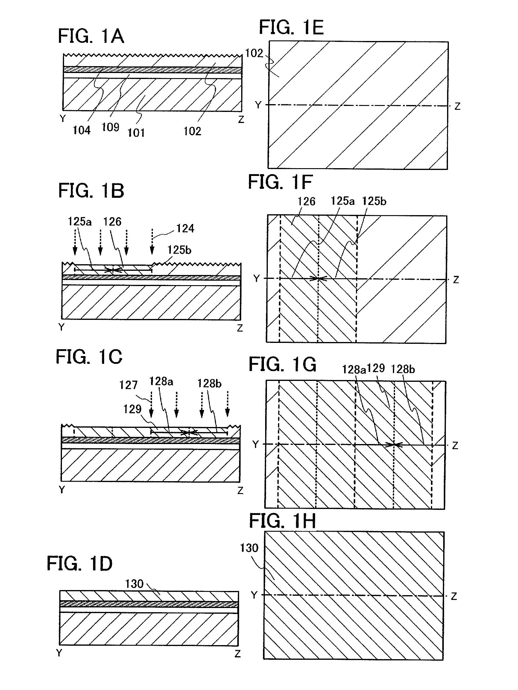
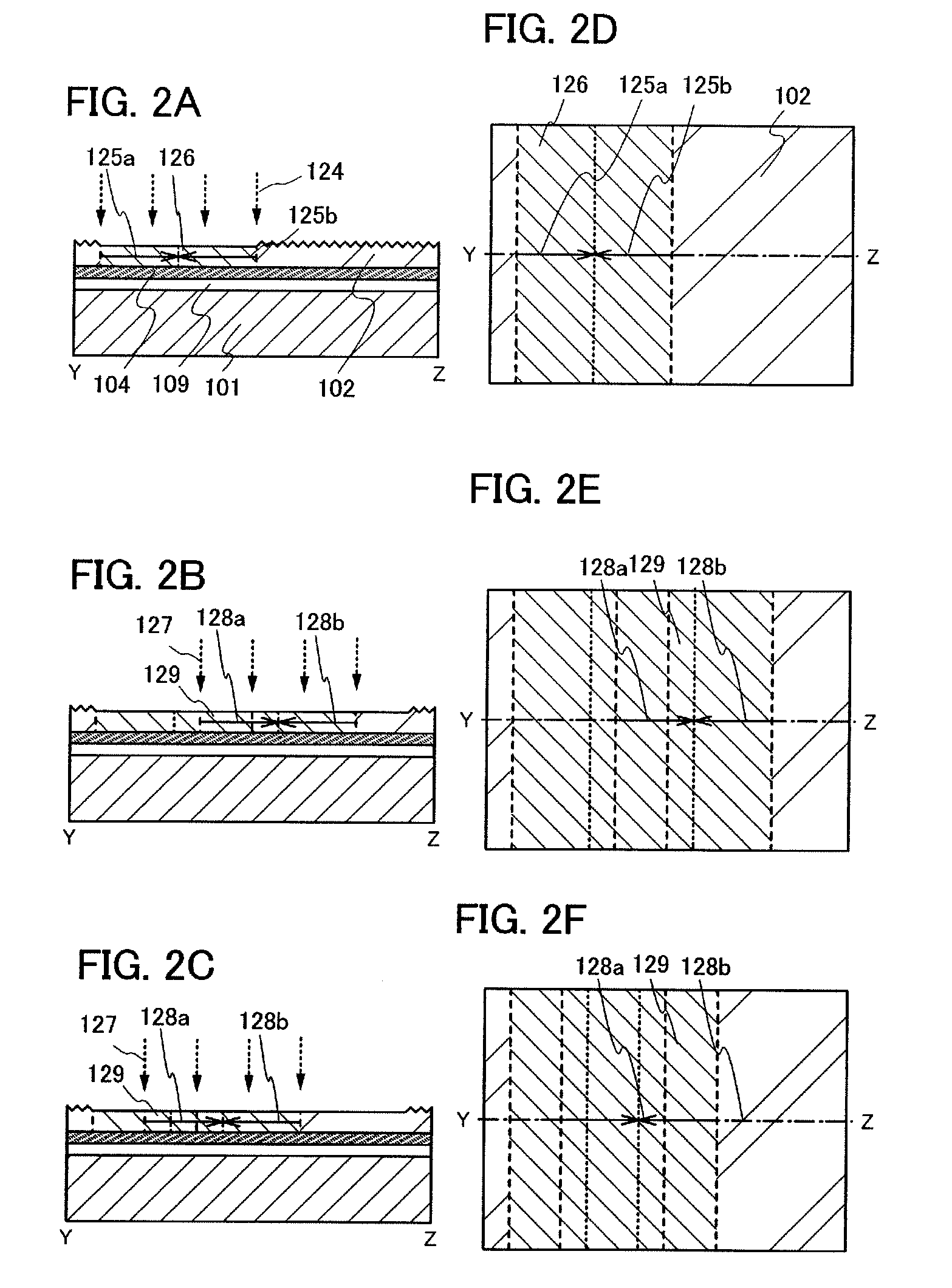
[0062]A method for manufacturing a semiconductor device of the present invention will be described with reference to FIGS. 1A to 1H, FIGS. 2A to 2F, FIGS. 3A to 3D and FIGS. 4A to 4C.
[0063]In this embodiment mode, in manufacturing a semiconductor substrate, pulsed laser light irradiation is performed for re-single-crystallization of a single crystal semiconductor layer which is separated from a single crystal semiconductor substrate and bonded to a supporting substrate having an insulating surface.
[0064]First, a method for providing a single crystal semiconductor layer from a single crystal semiconductor substrate over a supporting substrate having an insulating surface, will be described with reference to FIGS. 3A to 3D and FIGS. 4A to 4C.
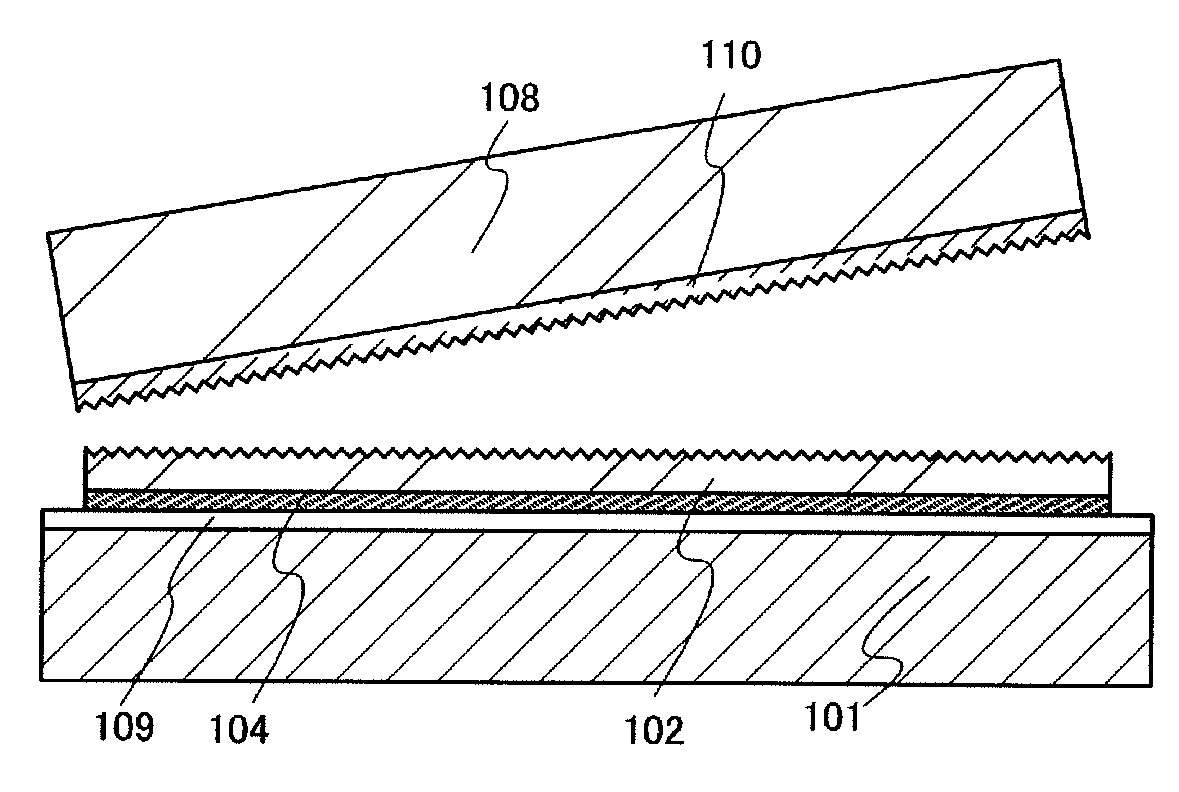
[0065]A single crystal semiconductor substrate 108 illustrated in FIG. 3A is cleaned, and ions accelerated by an electric field are added to reach a predetermined depth from the surface to form an embrittlement layer 110. The ions are added in con...
embodiment mode 2
[0186]This embodiment mode describes an example in which steps of separating a semiconductor layer from the single crystal semiconductor substrate and bonding the single crystal semiconductor layer to a supporting substrate are different from the steps in Embodiment Mode 1. Repetitive description of the same portion as or a portion having a similar function to the portions in Embodiment Mode 1 is omitted.
[0187]In this embodiment mode, when a single crystal semiconductor layer is transferred from a single crystal semiconductor substrate, the single crystal semiconductor substrate is selectively etched (this step is also referred to as groove processing) and a plurality of single crystal semiconductor layers of which shapes are processed are transferred to a supporting substrate. Thus, a plurality of island-shaped single crystal semiconductor layers can be formed over the supporting substrate. The single crystal semiconductor layers of which shapes are processed in advance are transfe...
embodiment mode 3
[0207]In this embodiment mode, a method for manufacturing a CMOS (complementary metal oxide semiconductor) device will be described as an example of a method for manufacturing a semiconductor device including a semiconductor element having high performance and high reliability with high yield with reference to FIGS. 7A to 7E and FIGS. 8A to 8D. Note that repetitive descriptions for the same components as or components having similar functions to the components in Embodiment Mode 1 are omitted.
[0208]In FIG. 7A, the blocking layer 109, the insulating layer 104, the protection layer 121, and the single crystal semiconductor layer 130 are formed over the supporting substrate 101. The single crystal semiconductor layer 130 corresponds to FIGS. 1(D1) and 1(D2); and the blocking layer 109, the insulating layer 104, and the protection layer 121 correspond to FIG. 4C. Note that here, although an example is shown in which a semiconductor substrate having a structure illustrated in FIG. 7A is ...
PUM
 Abstract
Description
Claims
Application Information