Semiconductor element, method for manufacturing same, wireless communication device, and sensor

Inactive Publication Date: 2019-04-04
TORAY IND INC
View PDF0 Cites 0 Cited by
  • Summary
  • Abstract
  • Description
  • Claims
  • Application Information

AI Technical Summary

Benefits of technology

[0018]According to the present invention, a semiconductor element having excellent switching characteristics, a wireless

Problems solved by technology

However, the manufacturing process of the inorganic semiconductor elements requires expensive manufacturing

Method used


Image

  • Semiconductor element, method for manufacturing same, wireless communication device, and sensor
  • Semiconductor element, method for manufacturing same, wireless communication device, and sensor
  • Semiconductor element, method for manufacturing same, wireless communication device, and sensor

Examples


example 1

[0159](1) Production of Semiconductor Solution

[0160]CNTs (1.5 mg) and P3HT (1.5 mg) were added to 15 mL of chloroform, and the mixture was stirred ultrasonically using an ultrasonic homogenizer (VCX-500, manufactured by TOKYO RIKAKIKAI CO, LTD.) at an output of 250 W for 30 minutes with being ice-cooled to produce a CNT dispersion A (the concentration of CNT composites in the solvent: 0.1 g / l).

[0161]Subsequently, a semiconductor solution for forming a semiconductor layer was produced. The CNT dispersion A was filtered using a membrane filter (pore diameter: 10 μm, diameter: 25 mm, Omnipore membrane manufactured by Millipore Corporation), and then further filtered using a membrane filter (pore diameter: 5 μm, diameter: 25 mm, Omnipore membrane manufactured by Millipore Corporation). o-DCB (45 mL) was added to 5 mL of the obtained filtrate to produce a semiconductor solution A (the concentration of CNT composites in the solvent: 0.01 g / l).

[0162](2) Production of Insulating Layer Solut...

example 2

[0173](1) Production of Semiconductor Element

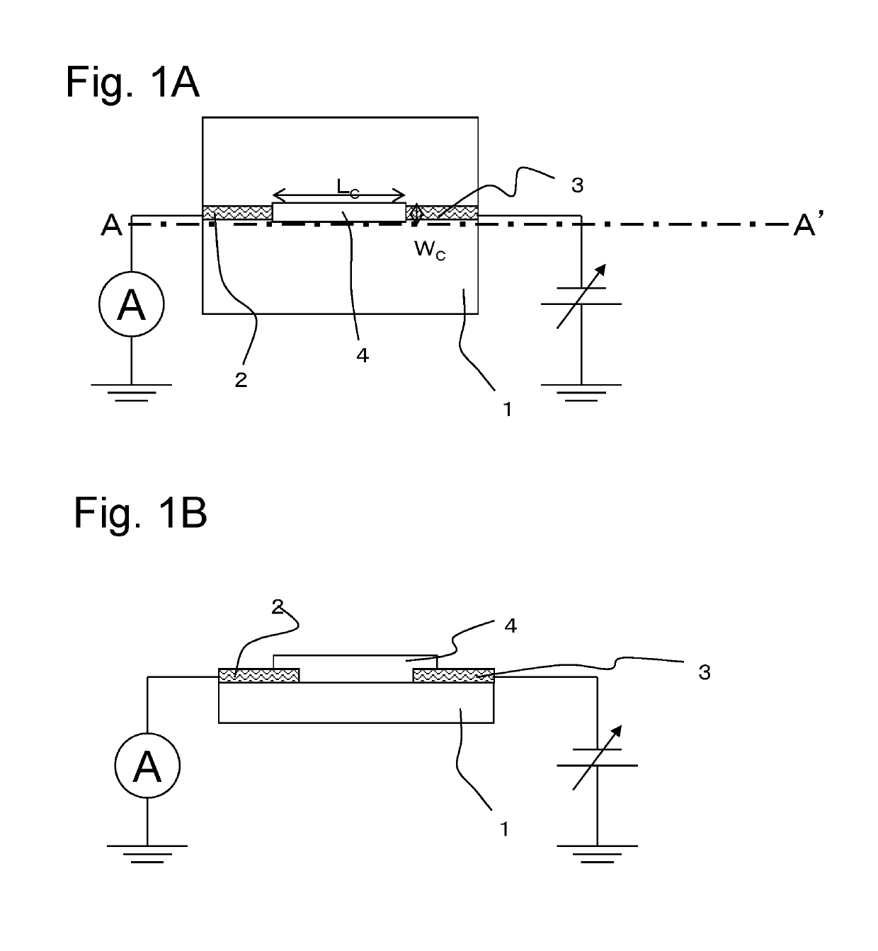
[0174]A semiconductor element was produced in the same manner as in Example 1 except that the channel length was 300 μm, and the semiconductor element in which the semiconductor layer 4 was modified with biotin, which is a biological substance that selectively interacts with a sensing target substance, and BSA as a protective agent was obtained.

[0175](2) Evaluation as Sensor

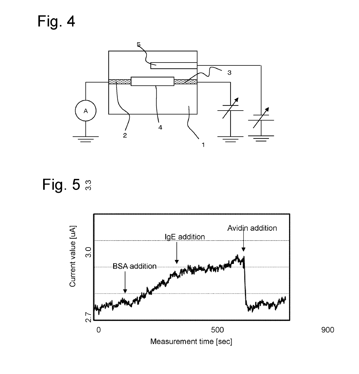
[0176]To evaluate the semiconductor element produced above as a sensor, measurement was carried out in the same manner as in Example 1. After 2 minutes of the start of measurement, 20 μL of 5 μg / mL BSA-0.01 M PBS solution, after 7 minutes, 20 μL of 5 μg / mL IgE-0.01 M PBS solution, and after 12 minutes, 20 μL of 5 μg / mL avidin-0.01 M PBS solution were added to 0.01 M PBS in which the semiconductor layer 4 was immersed. Only when avidin was added, the current value decreased by 7.1% from the current value before addition. The signal to noise ratio was 25.

example 3

[0177](1) Production of Semiconductor Element

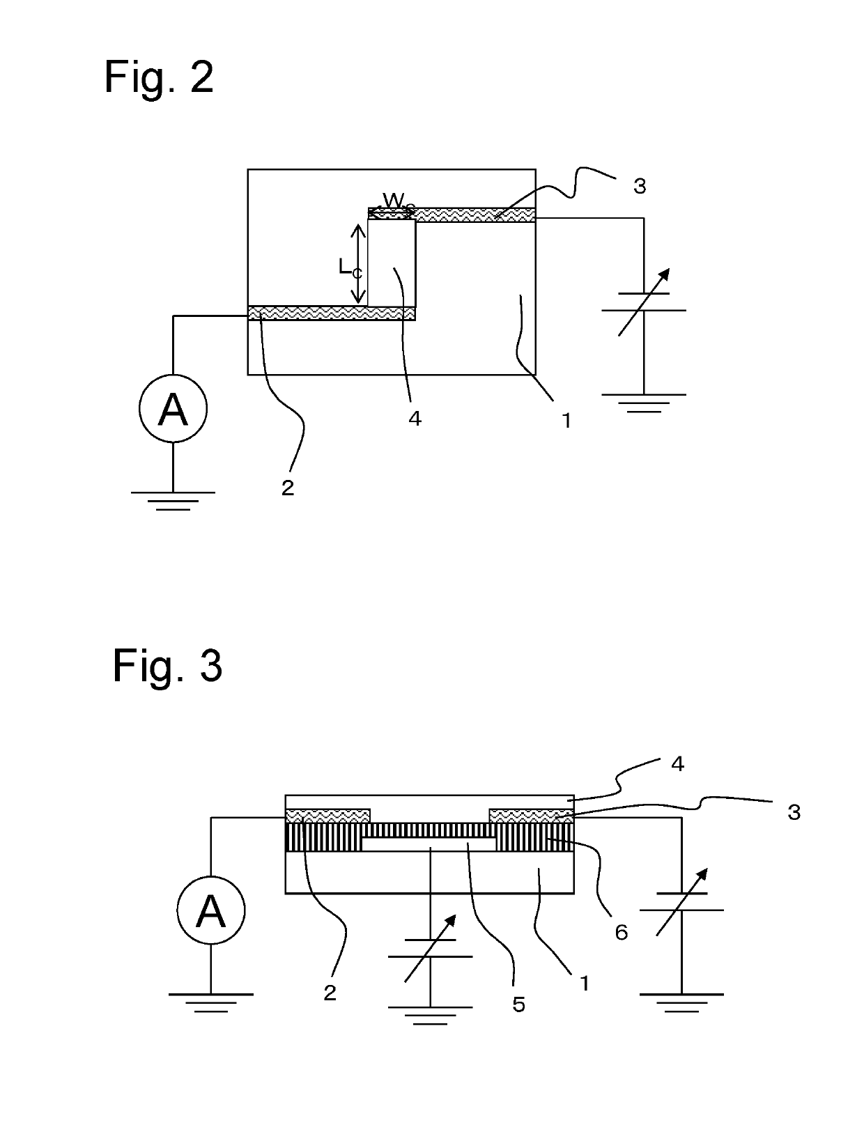
[0178]A semiconductor element was produced in the same manner as in Example 1 except that the channel length was 400 μm and 600 μL of the semiconductor solution A was dropped, and the semiconductor element in which the semiconductor layer 4 was modified with biotin, which is a biological substance that selectively interacts with a sensing target substance, and BSA as a protective agent was obtained.

[0179](2) Evaluation as Sensor

[0180]To evaluate the semiconductor element produced above as a sensor, measurement was carried out in the same manner as in Example 1. After 2 minutes of the start of measurement, 20 μL of 5 μg / mL BSA-0.01 M PBS solution, after 7 minutes, 20 μL of 5 μg / mL IgE-0.01 M PBS solution, and after 12 minutes, 20 μL of 5 μg / mL avidin-0.01 M PBS solution were added to 0.01 M PBS in which the semiconductor layer 4 was immersed. Only when avidin was added, the current value decreased by 8.0% from the current value before addi...


PUM

PropertyMeasurementUnit
Lengthaaaaaaaaaa
Percent by massaaaaaaaaaa

Abstract

A semiconductor element including a substrate, a first electrode, a second electrode, and a semiconductor layer disposed between the first electrode and the second electrode, wherein the semiconductor layer contains at least one selected from carbon nanotubes and graphene, and a relationship between a channel length LC and a channel width WC of the semiconductor element is 0.01≤WC/LC≤0.8. A semiconductor element having excellent switching characteristics and high detection sensitivity when used as a sensor is provided.

Description

TECHNICAL FIELD[0001]The present invention relates to a semiconductor element, a method for manufacturing the same, as well as a wireless communication device and a sensor including the semiconductor element.BACKGROUND ART[0002]Semiconductor elements such as transistors, memories, and capacitors are used in various electronic devices such as displays and computers utilizing their semiconductor characteristics. For example, IC tags and sensors that utilize electric characteristics of a field effect transistor (hereinafter referred to as a FET) have been developed.[0003]In recent years, for IC tags, a wireless communication system utilizing a RFID (Radio Frequency IDentification) technique has been developed for use as a contactless-type tag. In the RFID system, wireless communication is performed between a wireless transceiver called a reader / writer and a RFID tag. The RFID tag is expected to be used for various applications such as physical distribution management, product managemen...

Claims


Application Information

Patent Timeline
IPC IPC(8): G01N27/414H01L51/00H01L51/05H01L29/16H01L29/786
CPCG01N27/414H01L51/0048H01L51/0558H01L29/1606H01L29/786B82Y30/00G01N27/4145G01N27/4146B82Y15/00H10K85/221H10K85/113H10K10/484H10K10/00
Inventor ISOGAI, KAZUKIMURASE, SEIICHIRONAGAO, KAZUMASA
Owner TORAY IND INC
Why Eureka
Try Eureka