Semiconductor device, light emission element array, optical print head, and method of producing semiconductor device

Active Publication Date: 2018-02-01
OKI DATA CORP
View PDF9 Cites 0 Cited by
  • Summary
  • Abstract
  • Description
  • Claims
  • Application Information

AI Technical Summary

Benefits of technology

This patent describes a way to make a semiconductor device that has good contact between a layer of p-type material and an electrode. This results in better switching characteristics and prevents the need for more control currents. The method also allows for the simultaneous formation of two diffusion areas, simplifying the production process and reducing costs.

Problems solved by technology

As a result, switching characteristics of the light emission thyristor deteriorate and deterioration in characteristics such as an increase in gate current occurs.

Method used


Image

  • Semiconductor device, light emission element array, optical print head, and method of producing semiconductor device
  • Semiconductor device, light emission element array, optical print head, and method of producing semiconductor device
  • Semiconductor device, light emission element array, optical print head, and method of producing semiconductor device

Examples


first embodiment

First Embodiment

Light Emission Element Array 100

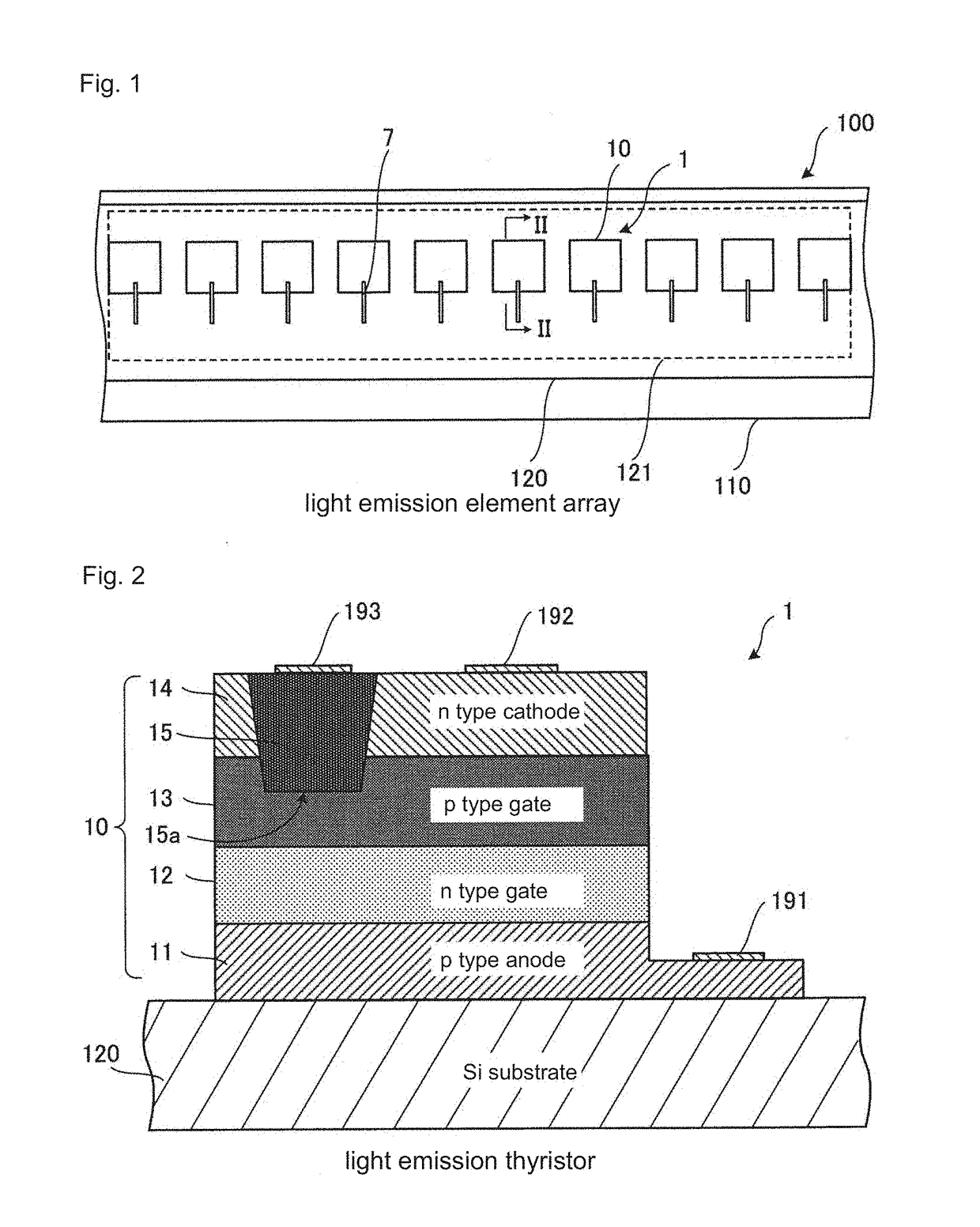
[0025]FIG. 1 is a plan view of a schematic structure of light emission element array 100 including semiconductor device 1 according to one or more embodiments. Light emission element array 100 is mounted on an optical print head as an exposure device in an electrophotographic image formation device. As illustrated in FIG. 1, light emission element array 100 includes, for example, chip on board (COB) substrate 110, semiconductor substrate 120 as a substrate mounted on COB substrate 110, and semiconductor devices 1 (light emission thyristors 10 as light emission elements) mounted on semiconductor substrate 120. Semiconductor substrate 120 and semiconductor devices 1 (light emission thyristors 10) form a light emission element array chip. Here, the optical print head is described in a sixth embodiment (to be described below).

[0026]Semiconductor substrate 120 is, for example, a silicon (Si) substrate, and incorporates drive circuit 121, ...

second embodiment

Second Embodiment

Semiconductor Device 2

[0042]FIG. 4 is a schematic cross-sectional view of a structure of semiconductor device 2 (light emission thyristor 20) according to a second embodiment. As illustrated in FIG. 4, semiconductor device 2 includes semiconductor substrate 220 as a substrate and light emission thyristor 20 that is provided on semiconductor substrate 220 and that is driven by a drive circuit.

[0043]As illustrated in FIG. 4, light emission thyristor 20 includes n type third semiconductor layer (n type cathode layer) 21 containing donors as impurities, p type first semiconductor layer (p type gate layer) 23 that is provided on n type cathode layer 21 and contains acceptors as impurities, n type second semiconductor layer (n type gate layer) 24 that is provided on p type gate layer 23 and contains donors, and p type first diffusion portion 25 which includes contact portion 25a in contact with p type gate layer 23 and in which contact portion 25a contains acceptors who...

third embodiment

Third Embodiment

Semiconductor Device 3

[0057]FIG. 6 is a schematic cross-sectional view of a structure of semiconductor device 3 (light emission thyristor 30) according to a third embodiment. As illustrated in FIG. 6, semiconductor device 3 according to the third embodiment includes semiconductor substrate 320 as a substrate and light emission thyristor 30 that is provided on semiconductor substrate 320 and that is driven by a drive circuit.

[0058]As illustrated in FIG. 6, semiconductor device 3 includes p type first semiconductor layer (p type gate layer) 33 containing acceptors as impurities, n type second semiconductor layer (n type cathode layer) 34 that is provided on p type gate layer 33 and contains donors as impurities, and p type first diffusion portion 35 which includes contact portion 35a in contact with p type gate layer 33 and in which contact portion 35a contains acceptors whose concentration is higher than that in p type gate layer 33. P type gate layer 33 includes fi...


PUM


Abstract

A semiconductor device includes: a p type first semiconductor layer that contains acceptors as impurities; an n type second semiconductor layer that is provided on the first semiconductor layer and contains donors as impurities; and a p type first diffusion portion that includes a contact portion in contact with the first semiconductor layer, the contact portion containing acceptors whose concentration is higher than that in the first semiconductor layer.

Description

CROSS REFERENCE TO RELATED APPLICATIONS[0001]This application claims priority based on 35 USC 119 from prior Japanese Patent Application No. 2016-148001 filed on Jul. 28, 2016, entitled “SEMICONDUCTOR DEVICE, LIGHT EMISSION ELEMENT ARRAY, OPTICAL PRINT HEAD, AND METHOD OF PRODUCING SEMICONDUCTOR DEVICE”, the entire contents of which are incorporated herein by reference.BACKGROUND1. Field[0002]The present disclosure relates to a semiconductor device, a light emission element array including light emission elements as semiconductor devices, an optical print head including a light emission element array, and a method of producing a semiconductor device.2. Description of Related Art[0003]An optical print head including a light emission thyristor array (a light emission element array) including light emission thyristors (light emission elements) is proposed as an exposure device for an electrophotographic image formation device (for example, refer to Patent Literature 1: Japanese Unexami...

Claims


Application Information

Patent Timeline
IPC IPC(8): H01L33/00H01L33/44G03G15/04H01L33/30H01L27/15H01L33/38H01L33/62
CPCH01L33/0016H01L33/38H01L33/44G03G15/04036H01L33/305H01L33/0062H01L27/15H01L33/62H01L25/0753H01L25/167H01L33/36H01L33/0093
Inventor FURUTA, HIRONORI
Owner OKI DATA CORP
Why Eureka
Try Eureka