Atomic layer deposition of metal oxides for memory applications

a metal oxide film and memory technology, applied in the field of memory devices, can solve the problems of insufficient resistance of low resistance metal oxide films to be used within a practical nonvolatile memory device, insufficient resistance of low resistance metal oxide films, and insufficient resistance of low resistance films to form reliable nonvolatile memory devices, etc., to achieve high aspect ratio, simple and accurate thickness control, excellent reproducibility and uniformity

Active Publication Date: 2013-02-07
SANDISK TECH LLC +2
View PDF6 Cites 36 Cited by
  • Summary
  • Abstract
  • Description
  • Claims
  • Application Information

AI Technical Summary

Benefits of technology

[0013]The described ALD processes are techniques for depositing ultra-thin metal oxide films due to practical advantages which includes simple and accurate thickness control, excellent reproducibility and uniformity, and capability to produce conformal films at sharp interfaces and trenches with high aspect ratio. By optimizing the ratio of metal precursor gas to oxidizer pulses, materials can be made metal rich or metal deficient, which in turn tailors the oxygen defect content and type (vacancy vs. interstitial), resulting in an enhancement or reduction in defect density to facilitate carrier transport. The former is a “softer” film or material which is more of a leaky film, whereas the latter constitutes a “harder” film or material which is less leaky film
[0014]Specifically designed “harder” (less leaky) metal oxide materials and films, such as stoichiometric hafnium oxide layers or films, may improve switching characteristics when used in combination with a “softer” (more leaky) metal oxide. An appropriately tailored version of hard metal oxide films could potentially resolve the tradeoff between easy breakdown of the soft metal oxide and providing better control of the switching currents for ReRAM device applications. The hard metal oxide materials and films in combination with the soft metal oxide materials and films, as described herein, are promising candidates as dielectric materials for the next-generation of ReRAM device applications.

Problems solved by technology

However, as device dimensions shrink, scaling issues are posing challenges for traditional nonvolatile memory technology.
Although metal oxide films such as these exhibit bistability, the resistance of these films and the ratio of the high-to-low resistance states are often insufficient to be of use within a practical nonvolatile memory device.
Therefore, a low resistance metal oxide film may not form a reliable nonvolatile memory device.
For example, in a nonvolatile memory that has conductive lines formed of a relatively high resistance metal such as tungsten, the resistance of the conductive lines may overwhelm the resistance of the metal oxide resistive switching element.
Therefore, the state of the bistable metal oxide resistive switching element may be difficult or impossible to sense.
Similar issues can arise from integration of the resistive switching memory element with current steering elements, such as diodes and / or resistors.
However, since the power that can be delivered to a circuit containing a series of resistive switching memory elements and current steering elements is typically limited in most conventional nonvolatile memory devices (e.g., CMOS driven devices), it is desirable to form each of the resistive switching memory elements and current steering elements in the circuit so that the voltage drop across each of these elements is small, and thus resistance of the series connected elements does not cause the current to decrease to an undesirable level due to the fixed applied voltage (e.g., about 2-5 volts).
However, these vapor deposition processes generally provide limited control to the thickness and the conformity of the deposited transition metal oxide films.
Often, CVD or PVD processes are incapable of forming conformal films at sharp interfaces and within trenches or vias having high aspect ratios.
The metal oxide films deposited by CVD often pinch-off and form voids within the high aspect ratio trenches and vias.
Also, the metal oxide films deposited by CVD generally suffer high concentrations of organic or halide contaminants.

Method used


Image

  • Atomic layer deposition of metal oxides for memory applications
  • Atomic layer deposition of metal oxides for memory applications
  • Atomic layer deposition of metal oxides for memory applications

Examples


Embodiment Construction

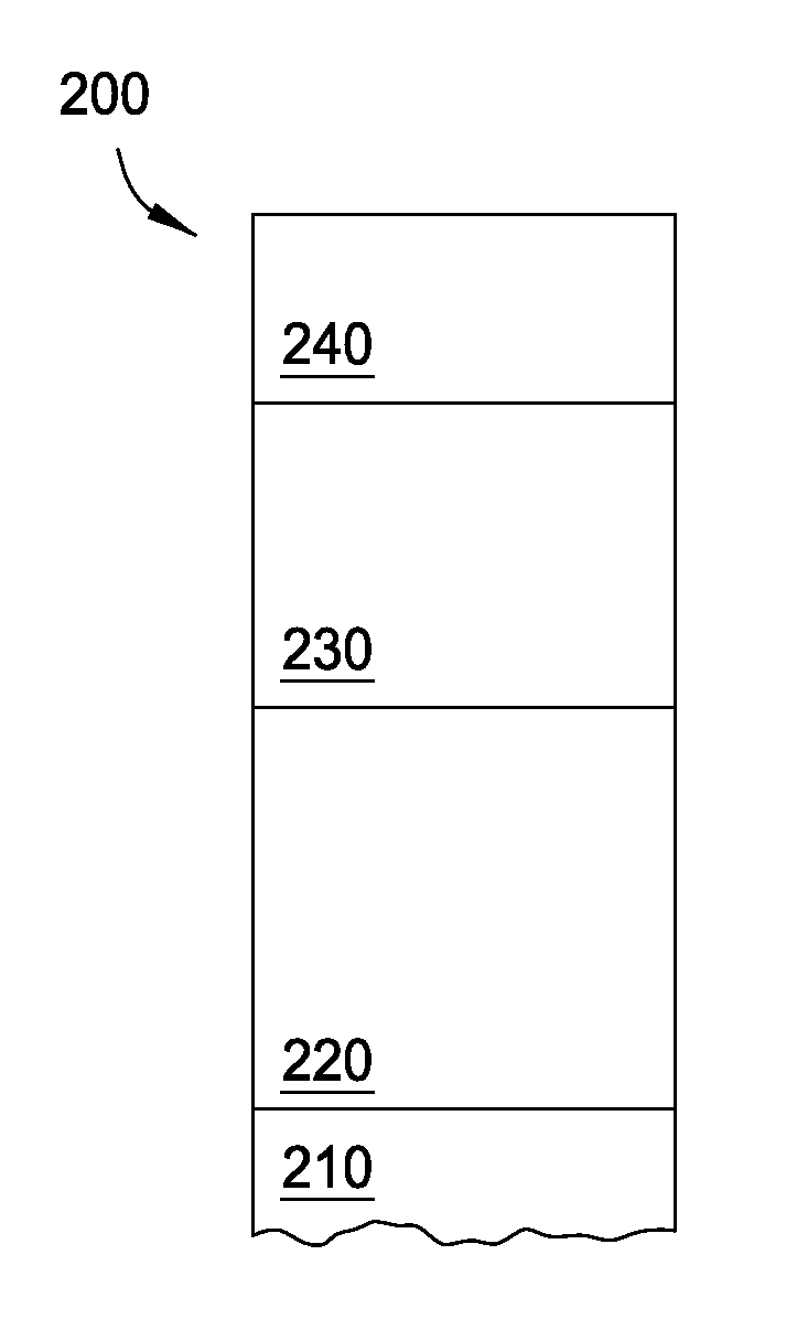
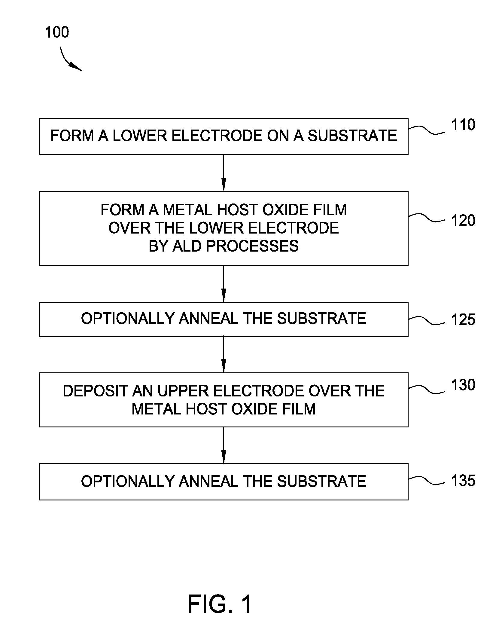
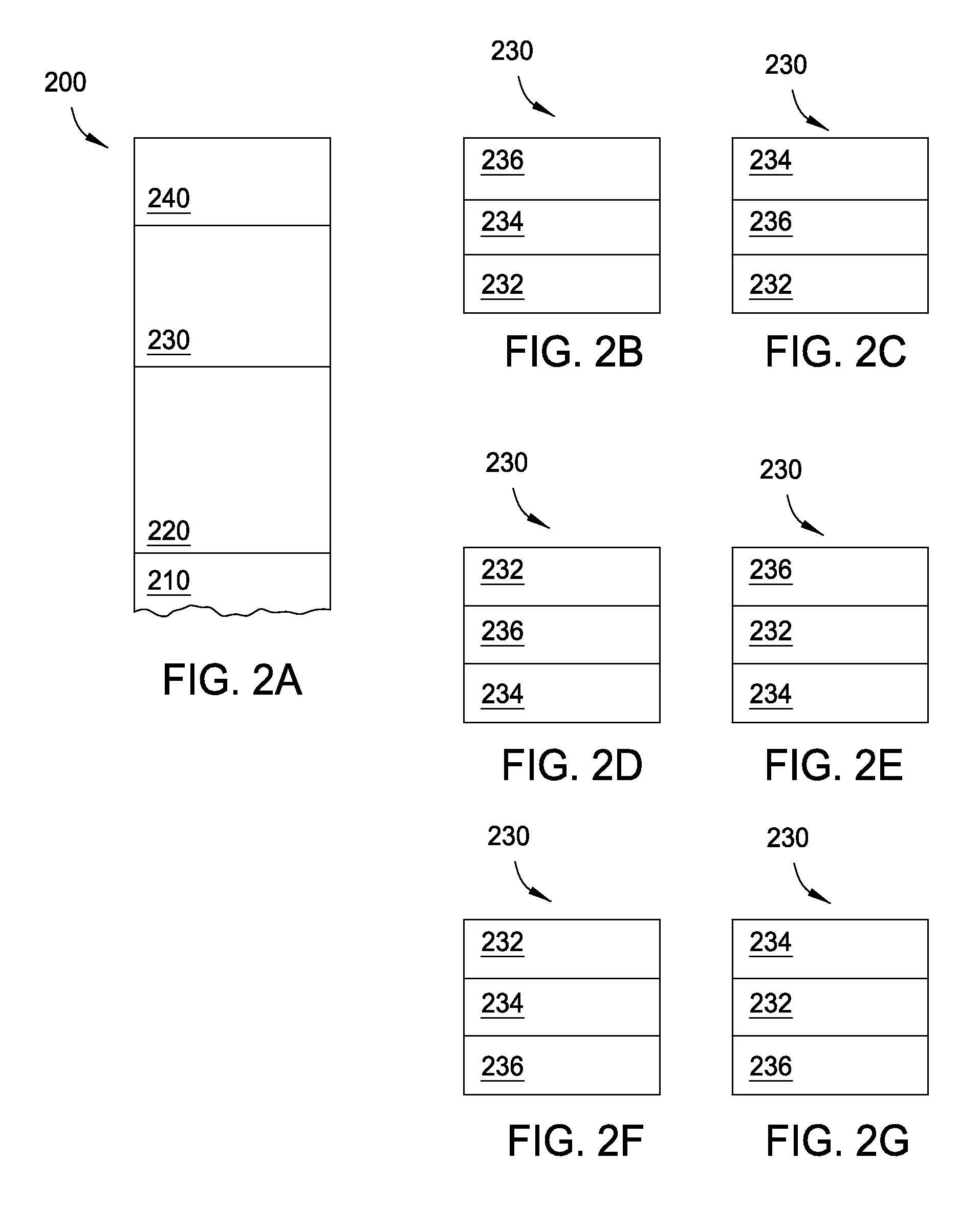
[0028]Embodiments of the invention generally relate to nonvolatile memory devices and methods for manufacturing such memory devices. The methods for forming improved memory devices, such as a ReRAM cells, provide optimized, atomic layer deposition (ALD) processes for making a metal oxide film stack containing one or more hard metal oxide films and one or more less resistive or soft metal oxide films. The hard metal oxide film is deposited by a hard ALD process (e.g., more oxidizing to metal) and may be disposed at the top or bottom of the metal oxide film stack. The metal source gas (e.g., TDMAHf) and the oxidizing agent (e.g., O3) may be sequentially pulsed into the chamber and exposed to the substrate, such that the metal source gas has a much longer pulse time relative to the pulse time used for the oxygen source gas during the hard ALD process. The soft metal oxide film may be deposited using a different or soft ALD process (e.g., less oxidizing to metal), whereas a different ox...


PUM

PropertyMeasurementUnit
temperatureaaaaaaaaaa
current leakageaaaaaaaaaa

Abstract

Embodiments of the invention generally relate to nonvolatile memory devices and methods for manufacturing such memory devices. The methods for forming improved memory devices, such as a ReRAM cells, provide optimized, atomic layer deposition (ALD) processes for forming a metal oxide film stack which contains at least one hard metal oxide film (e.g., metal is completely oxidized or substantially oxidized) and at least one soft metal oxide film (e.g., metal is less oxidized than hard metal oxide). The soft metal oxide film is less electrically resistive than the hard metal oxide film since the soft metal oxide film is less oxidized or more metallic than the hard metal oxide film. In one example, the hard metal oxide film is formed by an ALD process utilizing ozone as the oxidizing agent while the soft metal oxide film is formed by another ALD process utilizing water vapor as the oxidizing agent.

Description

BACKGROUND OF THE INVENTION[0001]1. Field of the Invention[0002]Embodiments of the invention generally relate to memory devices and methods for manufacturing such memory devices.[0003]2. Description of the Related Art[0004]Nonvolatile memory elements are used in systems in which persistent storage is required. For example, digital cameras use nonvolatile memory cards to store images and digital music players use nonvolatile memory to store audio data. Nonvolatile memory is also used to persistently store data in computer environments. Nonvolatile memory is often formed using electrically-erasable programmable read only memory (EPROM) technology. This type of nonvolatile memory contains floating gate transistors that can be selectively programmed or erased by application of suitable voltages to their terminals.[0005]As fabrication techniques improve, it is becoming possible to fabricate nonvolatile memory elements with increasingly smaller dimensions. However, as device dimensions sh...

Claims


Application Information

Patent Timeline
Patent Type & Authority Applications(United States)
IPC IPC(8): H01L21/20B82Y40/00
CPCH01L45/04H01L27/2463H01L45/1616H01L45/146H10B63/80H10N70/20H10N70/023H10N70/8833H10N70/24H10N70/826
Inventor HONG, ZHENDONGPHAM, HIEUHIGUCHI, RANDALLGOPAL, VIDYUTHASHIM, IMRAN
Owner SANDISK TECH LLC
Why Eureka
Try Eureka