Pixel circuit, active matrix apparatus and display apparatus

a technology of active matrix and display apparatus, which is applied in the direction of electric variable regulation, process and machine control, instruments, etc., can solve the problems of difficult high definition and large size of display apparatus, and achieve the effect of reducing the cost of tft substra

Inactive Publication Date: 2007-05-10
SONY CORP
View PDF21 Cites 248 Cited by
  • Summary
  • Abstract
  • Description
  • Claims
  • Application Information

AI Technical Summary

Benefits of technology

[0013] While the pixel circuit shown in FIG. 11 is formed using a p-channel TFT, if it can be formed otherwise using an n-channel TFT, then a conventional amorphous silicon (a-Si) process can be applied to TFT production. This makes it possible to reduce the cost of a TFT substrate, and it is expected to develop a pixel circuit formed using an n-channel TFT.
[0020] Therefor, it is desirable to provide a pixel circuit by which the luminance of light to be emitted can be kept fixed even if the I-V characteristic of a load element of the current driven type (an electro-optical element such as, for example, an organic EL element) such as a light emitting element varies with time.
[0021] It is also desirable to provide a pixel circuit wherein a load element can be driven stably even if the threshold voltage of a transistor which forms the pixel circuit varies with time.
[0029] According to certain embodiments of the present invention, the pixel circuit includes an electro-optical element, a holding capacitor, a sampling transistor, a drive transistor, a switching transistor, a first detection transistor and a second detection transistor. The pixel circuit has a bootstrap function of the holding capacitor, and therefore, even if the I-V characteristic of an electro-optical element of a current driven type such as a light emitting element varies with time, the luminance of light emission can be kept fixed. Further, the threshold voltage of the drive transistor is detected by the first and second detection transistors, and the variation of the threshold voltage of the drive transistor is compensated for by the circuit means. Consequently, the electro-magnetic element can be driven stably. Particularly, the pixel circuit has a reasonable configuration which includes a minimized number of circuit elements. As the number of component elements is small, the yield is enhanced and reduction in cost can be anticipated.

Problems solved by technology

The former has a problem that implementation of a display apparatus of a large size and a high definition is difficult although it is simple in structure.

Method used


Image

  • Pixel circuit, active matrix apparatus and display apparatus
  • Pixel circuit, active matrix apparatus and display apparatus
  • Pixel circuit, active matrix apparatus and display apparatus

Examples


Embodiment Construction

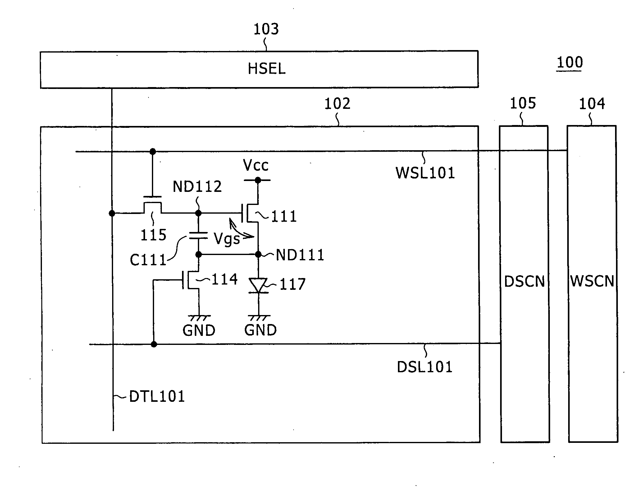
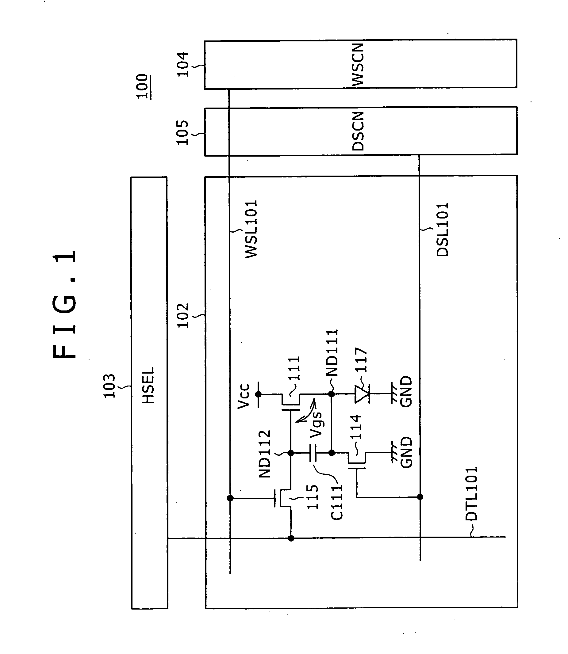
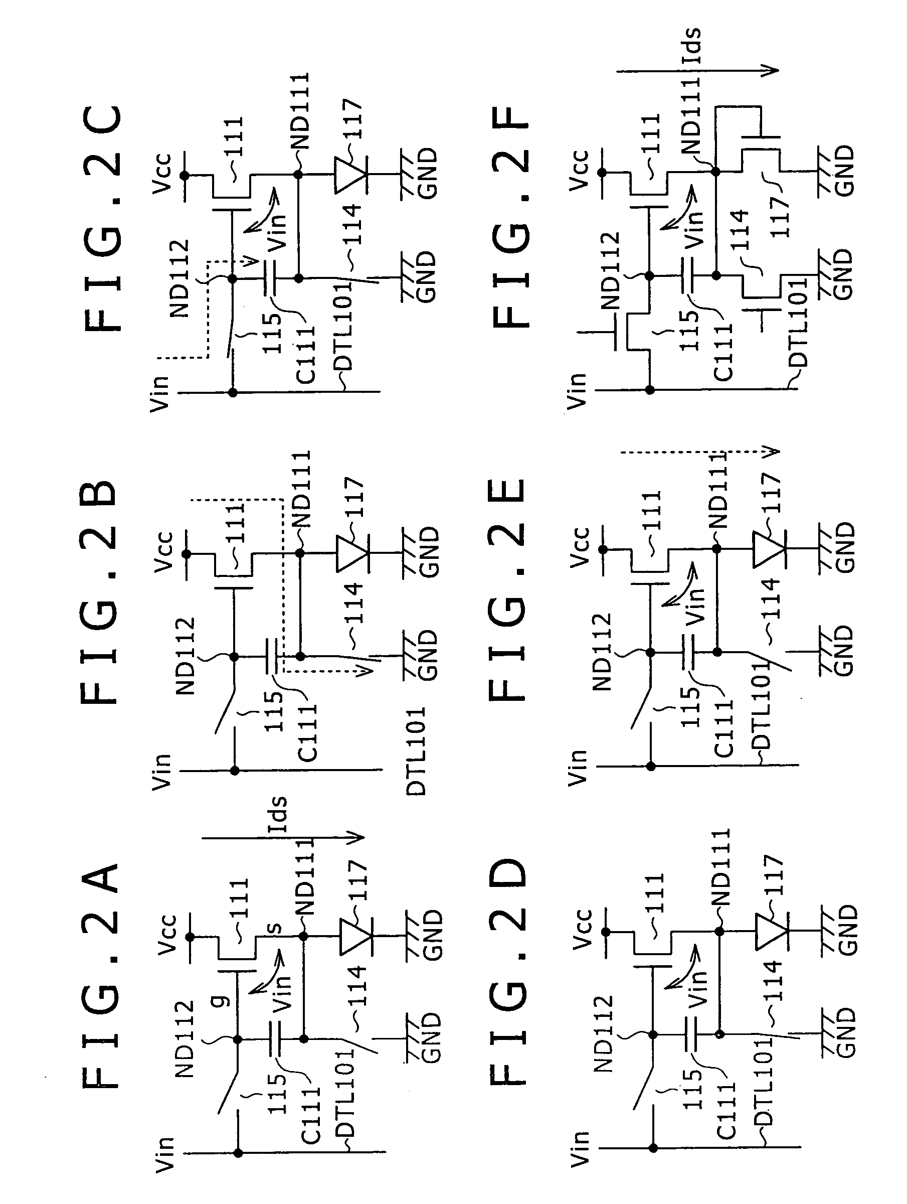
[0046] Now, preferred embodiments of the present invention are described in detail with reference to the accompanying drawings. For the convenience of description, a pixel circuit which has a characteristic variation compensation function (bootstrap function) of a light emitting element serving as a load element is described first, and then, another pixel circuit which additionally has a threshold voltage variation compensation function of a drive transistor is described. Thereafter, further pixel circuits which have such compensation functions as mentioned above while they are composed of a minimized number of circuit components are described. FIG. 1 shows a configuration of a display apparatus which includes a pixel circuit having a bootstrap function which is a compensation function for a characteristic variation of a light emitting element which is an electro-optical element. It is to be noted that the circuit configuration shown in FIG. 1 is disclosed in Japanese Patent Applica...


PUM


Abstract

A pixel circuit having a function of compensating for characteristic variation of an electro-optical element and threshold voltage variation of a transistor is formed from a reduced number of component elements. The pixel circuit includes an electro-optical element, a holding capacitor, a sampling transistor, a drive transistor, a switching transistor, and first and second detection transistors. The sampling transistor samples and supplies an input signal from a signal line so as to be held into the holding capacitor. The driving transistor drives the electro-optical element with current in response to the held signal potential. The first and second detection transistors supply a threshold voltage of the drive transistor into the holding capacitor in order to cancel an influence of the threshold voltage in advance.

Description

CROSS REFERENCE TO RELATED APPLICATIONS [0001] This application is a continuation of application Ser. No. 11 / 140,199, entitled “Pixel Circuit, Active Matrix Apparatus and Display Apparatus, filed on May 31, 2005, which claims priority under 35 U.S.C. 119 to 2004-164681 and 2004-164682, both filed in Japan on Jun. 2, 2004. The entire contents of these applications are hereby incorporated by reference.BACKGROUND OF THE INVENTION [0002] This invention relates to a pixel circuit wherein a load element disposed for each pixel is driven by current and also to a matrix apparatus wherein a plurality of pixel circuits are disposed in a matrix and particularly to an active matrix apparatus wherein an amount of current to be supplied to a load element is controlled by an insulating gate type field effect transistor provided in each pixel circuit. The present invention further relates to a display apparatus of the active matrix type which includes an electro-optical element whose luminance is c...

Claims


Application Information

Patent Timeline
Patent Type & Authority Applications(United States)
IPC IPC(8): G09G3/36G09G3/10
CPCG09G3/2011G09G3/3233G09G3/3291G09G2300/0417G09G2300/0809G09G2300/0819G09G2300/0842G09G2300/0852G09G2300/0861G09G2310/0216G09G2310/0256G09G2310/0267G09G2320/043G09G3/20G09G3/30G02B6/4214G02B6/4268G02B6/4272G09G3/3258G09G3/3266G09G2320/045G09G2320/0626G09G2320/0633G09G2330/021H01L2224/16225H01L2924/15192H01L2924/15311H04B10/501
Inventor UCHINO, KATSUHIDEYAMASHITA, JUNICHIYAMAMOTO, TETSURO
Owner SONY CORP
Why Eureka
Try Eureka