
Image signal processing device, imaging device, and image signal processing method

Active Publication Date: 2007-05-10
SONY SEMICON SOLUTIONS CORP
View PDF3 Cites 42 Cited by
  • Summary
  • Abstract
  • Description
  • Claims
  • Application Information

AI Technical Summary

Benefits of technology

[0026] It is thus desirable to provide an image signal processing device, an imaging device, and an image signal processing method, all implementing an adoptive (dynamic) change of a frame rate in accordance with an amount of motion, and image recording in rapid succession, enabling smooth recording of moving images, and recording of still images following a fast-moving object.
[0038] According to the embodiments of the invention, a frame rate can be changed adoptively (dynamically) in accordance with an amount of motion, and image recording in rapid succession, enabling smooth recording of moving images, and recording of still images following a fast-moving object can be implemented.

Problems solved by technology

As such, to achieve a reduction of the amount of recording data using the previous technology, there are problems as described below.

Method used


Image

  • Image signal processing device, imaging device, and image signal processing method
  • Image signal processing device, imaging device, and image signal processing method
  • Image signal processing device, imaging device, and image signal processing method

Examples


first embodiment

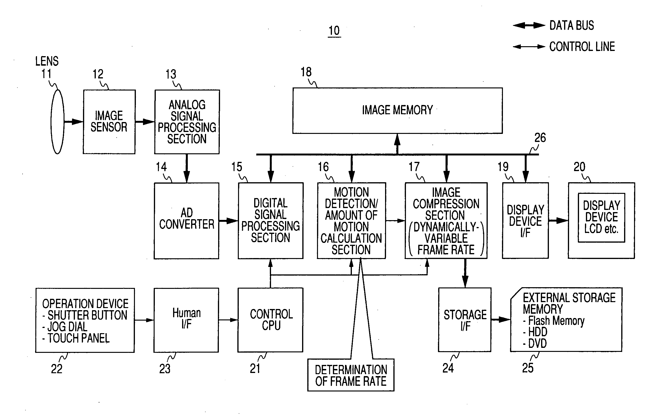
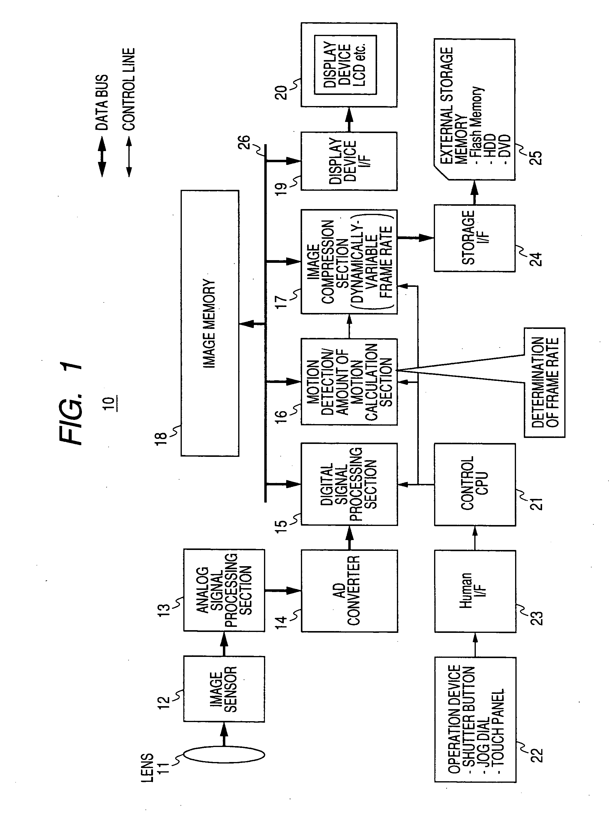
[0051]FIG. 1 is a block diagram showing an exemplary configuration of a camera system (imaging device) equipped with an image signal processing device of the invention.

[0052] A camera system 10 is configured to include an optical system 11, an image sensor (imaging device) 12, an analog signal processing section 13, an analog / digital (A / D) converter 14, a digital signal processing section 15, a motion detection / amount of motion calculation section 16, an image compression / decompression section 17, an image memory 18, a display device interface (I / F) 19, a display device 20, a control CPU (Central Processing Unit) 21, an operation device 22, a human I / F 24, a storage I / F 24, and an external storage memory 25 serving as a recording section. The image sensor 12 is exemplified by a CCD (Charge-Coupled Device) or a CMOS (Complementary Metal Oxide Semiconductor) sensor. The motion detection / amount of motion calculation section 16 serves as a first processing section, and the image compres...

second embodiment

[0108]FIG. 8 is a block diagram showing an exemplary configuration of a camera system of the invention.

[0109] A camera system 10A of the second embodiment is different from the camera system 10 of the first embodiment in the respect that an image sensor 12A is made controllable by a CPU 21A so that a frame rate is automatically increased.

[0110] More specifically, the camera system 10A is substantially similar in basic configuration to the system of FIG. 1, has the functions of capturing images with a high frame rate, calculating the amount of frame-to-frame motion, and summing and storing the amount of motion at each frame, and has a data area for temporary storage of a high-frame-rate imaging data of a fixed length of time. The high-frame-rate imaging operation is autonomously started when the sum amount of motion derived for any captured image reaches a fixed value, thereby implementing the function of capturing, with reliability, any object with a large amount of motion even if ...


PUM


Abstract

An image signal processing device that includes: a recording section; a first processing section that calculates an amount of screen motion through detection of a motion of a captured image, and determines a frame rate through comparison between the amount of screen motion and a preset motion threshold value; and a second processing section that performs recording of the captured image to the recording section using the dynamically-variable frame rate notified by the first processing section.

Description

CROSS REFERENCES TO RELATED APPLICATIONS [0001] The present invention contains subject matter related to Japanese Patent Application JP 2005-326413 filed in the Japanese Patent Office on Nov. 10, 2005, the entire contents of which being incorporated herein by reference. BACKGROUND OF THE INVENTION [0002] 1. Field of the Invention [0003] The present invention relates to an image signal processing device that processes a succession of images, an imaging device, and an image signal processing method. [0004] 2. Description of the Related Art [0005] As to a succession of images, the amount of processing data is generally proportional to a frame rate. [0006] Recording a succession of high-frame-rate images with a previous method requires a large amount of recording data. There is thus a demand for a recording method enabling a further reduction of an amount of recording data. [0007] The recording method for capturing a succession of images is mainly classified into two types as follows: [...

Claims


Application Information

Patent Timeline
IPC IPC(8): H04N7/26H04N5/225H04N5/232H04N5/92
CPCH04N19/503H04N19/172H04N19/15H04N19/587H04N19/137H04N19/152H04N19/132
Inventor SAITO, MASATAKEEMOTO, NOBUYA
Owner SONY SEMICON SOLUTIONS CORP
Learn More