Light-emitting device having light-emitting elements

a technology of light-emitting devices and light-emitting elements, which is applied in the direction of diodes, electronic switching, pulse techniques, etc., can solve the problem of not being able to increase the drive voltage sufficiently, and achieve the effect of high drive voltag

Inactive Publication Date: 2007-06-21
SEOUL SEMICONDUCTOR
View PDF43 Cites 22 Cited by
  • Summary
  • Abstract
  • Description
  • Claims
  • Application Information

AI Technical Summary

Benefits of technology

[0004] An object of the present invention is to provide a light emitting device which can be operated with a high drive voltage.
[0016] Various methods are available for two-dimensionally placing or arranging a plurality of light emitting elements, and a method which minimizes an area occupied on the substrate is desirable. For example, by arranging the two groups of light emitting element arrays in zigzag pattern, that is, arranging a plurality of light emitting elements on a bent line and alternately arranging the light emitting element arrays, the substrate area can be efficiently utilized and a large number of light emitting elements can be connected. When the two light emitting element arrays are alternately positioned, a crossing portion of lines may occur. It is possible to effectively prevent short-circuiting at the crossing portion by connecting the light emitting elements by air bridge lines. The shapes of the light emitting elements and the electrodes is not limited. By forming the light emitting elements and the electrodes to have a planar shape of, for example, approximate square, the overall shape becomes an approximate square, which allows for the use of a standard mounting structure. It is also possible to employ a shape other than the square, for example, a triangle, for the light emitting elements and the electrodes, to form an approximate square shape as an overall shape by combining the triangles, and, as a consequence, it is possible to use a standard mounting structure in a similar manner.

Problems solved by technology

In the LEDs of the related art, however, it is not always possible to sufficiently increase the drive voltage.

Method used


Image

  • Light-emitting device having light-emitting elements
  • Light-emitting device having light-emitting elements
  • Light-emitting device having light-emitting elements

Examples


Embodiment Construction

[0048] A preferred embodiment of the present invention will now be described referring to the drawings.

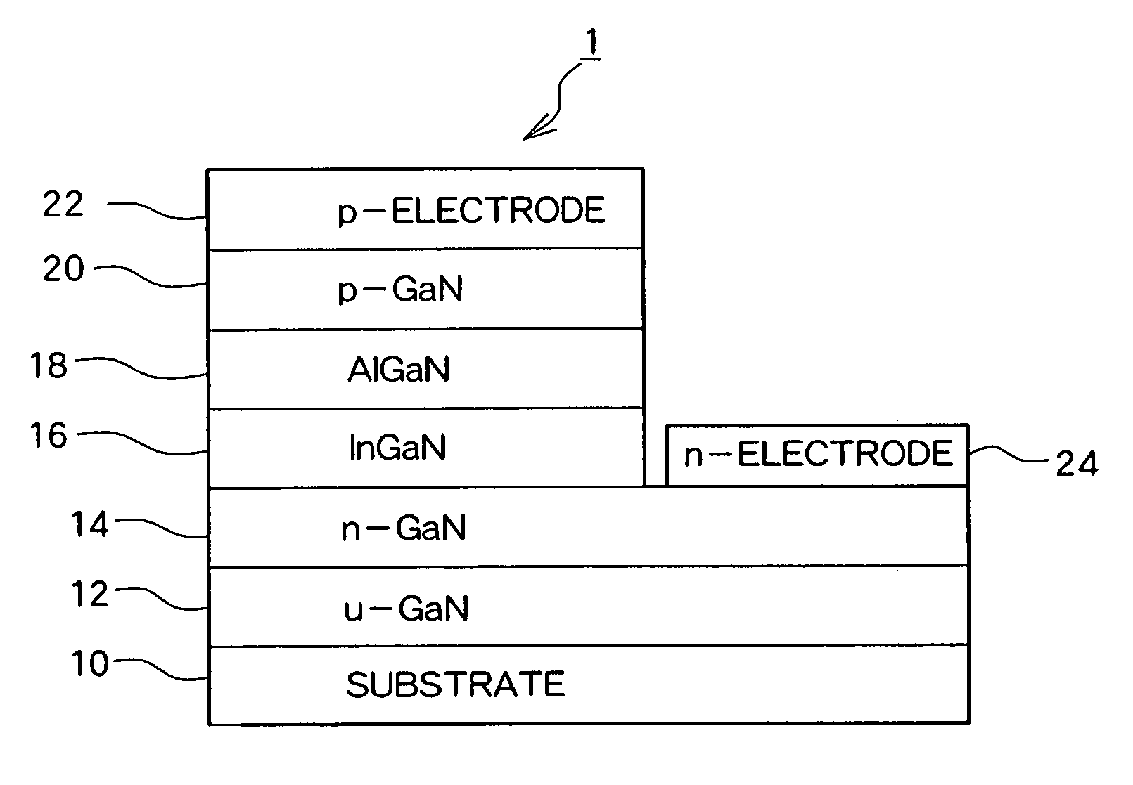
[0049]FIG. 1 shows a basic structure of an LED 1 which is a GaN-based compound semiconductor light emitting element of the present embodiment. The LED 1 has a structure in which a GaN layer 12, an Si-doped n-type GaN layer 14, an InGaN light emitting layer 16, an AlGaN layer 18, and a p-type GaN layer 20 are sequentially layered on a substrate 10, a p electrode 22 is formed in contact with the p-type GaN layer 20, and an n electrode 24 is formed in contact with the n-type GaN layer 14.

[0050] The LED shown in FIG. 1 is manufactured through the following process. First, a sapphire c-plane substrate is thermally treated for 10 minutes in a hydrogen atmosphere at a temperature of 1100° C. in an MOCVD device. Then, the temperature is reduced to 500° C. and silane gas and ammonia gas are supplied for 100 seconds to form a discontinuous SiN film on the substrate 10. This process is appl...


PUM


Abstract

A light-emitting device operating on a high drive voltage and a small drive current. LEDs (1) are two-dimensionally formed on an insulating substrate (10) of e.g., sapphire monolithically and connected in series to form an LED array. Two such LED arrays are connected to electrodes (32) in inverse parallel. Air-bridge wiring (28) is formed between the LEDs (1) and between the LEDs (1) and electrodes (32). The LED arrays are arranged zigzag to form a plurality of LEDs (1) to produce a high drive voltage and a small drive current. Two LED arrays are connected in inverse parallel, and therefore an AC power supply can be used as the power supply.

Description

TECHNICAL FIELD [0001] The present invention relates to a light emitting device in which a plurality of light emitting elements are formed on a substrate. BACKGROUND ART [0002] When light emitting means such as a light emitting element (LED) is used for display or the like, typical usage conditions are approximately 1 V to 4 V for the drive voltage and approximately 20 mA for the drive current. With the recent development of short-wavelength LEDs which uses a GaN-based compound semiconductor and commercialization of solid light sources of full color, white color, etc., application of LEDs for illumination purposes has been considered. When an LED is used for illumination, there may be cases in which the LED is used under conditions other than the above-described conditions of 1 V-4 V of drive voltage and 20 mA of drive current. As a result, steps have been taken to enable a larger current to flow through the LED and to increase the light emission output. In order to flow a larger cu...

Claims


Application Information

Patent Timeline
Patent Type & Authority Applications(United States)
IPC IPC(8): H01L33/00H01L25/075H01L27/15H01L33/02H01L33/32H01L33/36H01L33/62
CPCH01L33/38H01L33/62H01L33/32H01L27/156H01L33/20H01L27/15H01L27/153H01L2224/24H01L33/08H01L33/42
Inventor SAKAI, SHIROAO, JIN-PINGONO, YASUO
Owner SEOUL SEMICONDUCTOR
Why Eureka
Try Eureka