

Efficient electroluminescent device
a technology of electroluminescent devices and organic light-emitting diodes, which is applied in the direction of discharge tubes/lamp details, luminescnet screens, natural mineral layered products, etc., can solve the problems of insufficient color purity and el efficiency of oled materials in an oled, a large range of oled applications, and a large amount of oled applications, etc., to achieve the effect of improving the drive voltag
- Summary
- Abstract
- Description
- Claims
- Application Information
AI Technical Summary
Benefits of technology
Problems solved by technology
Method used
Image

Examples
example 1
EL Device Fabrication
Inventive Examples
[0176] Sample Preparation and Testing
[0177] EL devices satisfying the requirements of the invention as Sample 1-2 and Comparatives were constructed in the following manner:
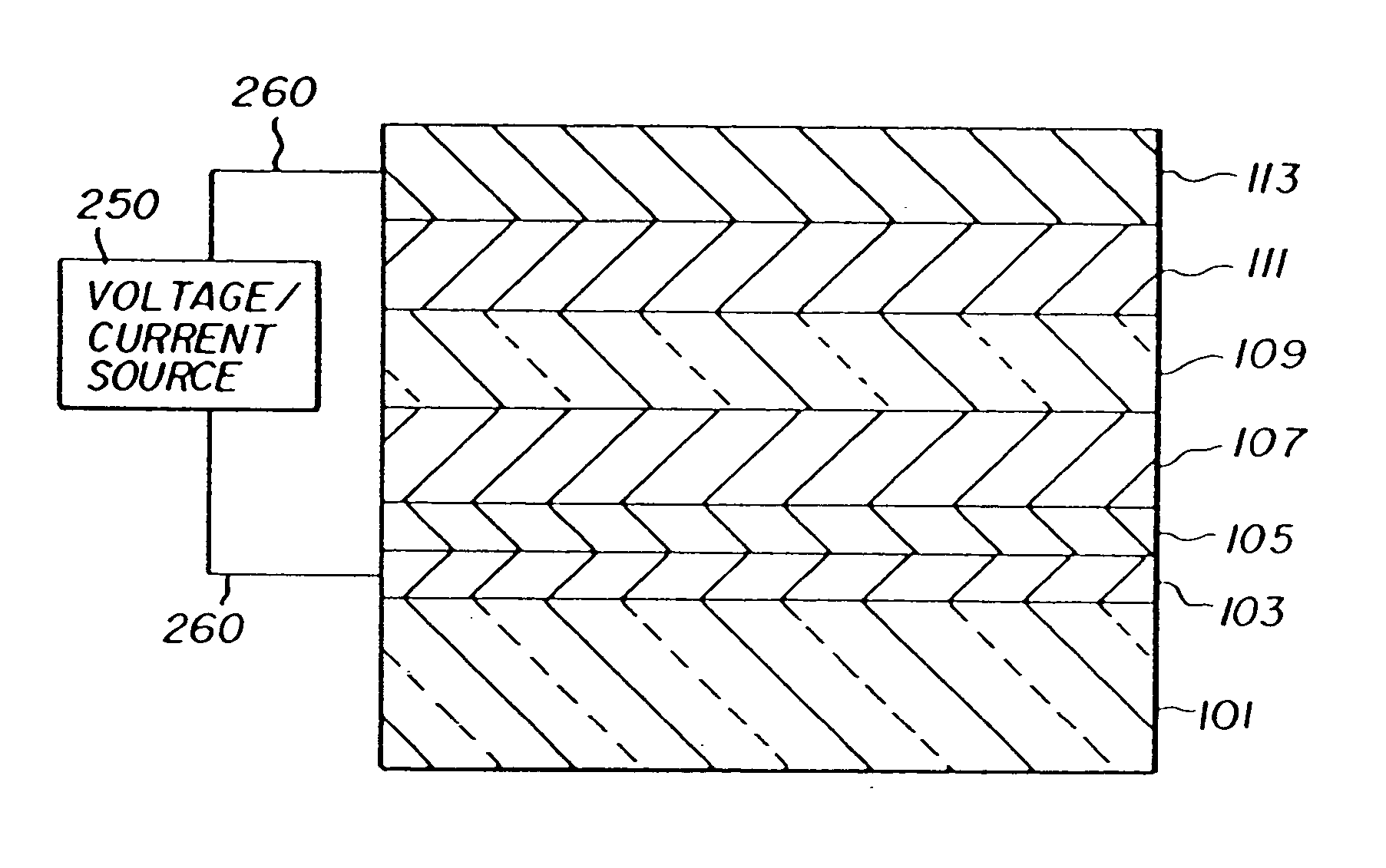
[0178] A glass substrate coated with an 85 nm layer of indium-tin oxide (ITO) as the anode was sequentially ultrasonicated in a commercial detergent, rinsed in deionized water, degreased in toluene vapor and exposed to oxygen plasma for about 1 min.
[0179] a) Over the ITO was deposited a 1 nm fluorocarbon (CFx) hole-injecting layer (HIL) by plasma-assisted deposition of CHF3.
[0180] b) A hole-transporting layer (HTL) of N,N′-di-1-naphthalenyl-N,N′-diphenyl-4,4′-diaminobiphenyl (NPB) having a thickness of 75 nm was then evaporated from a tantalum boat.
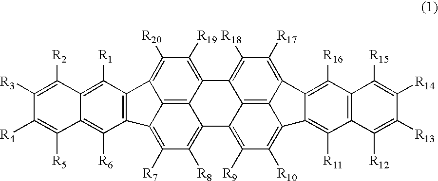
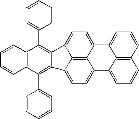
[0181] c) A 37.5-65.8 nm LEL comprised of tris(8-quinolinolato)aluminum (III) (Inv-23, 0-99.5 wt %), 9,10,11,12-tetraphenylnaphthacene (Inv-16, 0-99.5 wt %) and emitter-electroluminescent component, Inv-1, (0.27-0.50 wt %) w...
example 2
EL Device Fabrication
Inventive Examples
[0189] Sample Preparation and Testing
[0190] EL devices satisfying the requirements of the invention as Sample 4 and as Comparatives were constructed in the following manner:
[0191] A glass substrate coated with an 85 nm layer of indium-tin oxide (ITO) as the anode was sequentially ultrasonicated in a commercial detergent, rinsed in deionized water, degreased in toluene vapor and exposed to oxygen plasma for about 1 min.
[0192] a) Over the ITO was deposited a 1 nm fluorocarbon (CFx) hole-injecting layer (HIL) by plasma-assisted deposition of CHF3.
[0193] b) A hole-transporting layer (HTL) of N,N′-di-1-naphthalenyl-N,N′-diphenyl-4,4′-diaminobiphenyl (NPB) having a thickness of 75 nm was then evaporated from a tantalum boat.
[0194] c) A 37.5-67.2 nm LEL comprised of tris(8-quinolinolato)aluminum (III) (Inv-23, 0-99.5 wt %), 9,10,11,12-tetraphenylnaphthacene (Inv-16, 0-99.5 wt %) and emitter-electroluminescent component, Inv-1, (0.30-0.50 wt %) ...
example 3
EL Device Fabrication
Inventive Examples
[0200] Sample Preparation and Testing
[0201] EL devices satisfying the requirements of the invention as Samples 5-8 and Comparatives were constructed in the following manner:
[0202] A glass substrate coated with an 85 nm layer of indium-tin oxide (ITO) as the anode was sequentially ultrasonicated in a commercial detergent, rinsed in deionized water, degreased in toluene vapor and exposed to oxygen plasma for about 1 min.
[0203] a) Over the ITO was deposited a 1 nm fluorocarbon (CFx) hole-injecting layer (HIL) by plasma-assisted deposition of CHF3.
[0204] b) A hole-transporting layer (HTL) of N,N′-di-1-naphthalenyl-N,N′-diphenyl-4,4′-diaminobiphenyl (NPB) having a thickness of 75 nm was then evaporated from a tantalum boat.
[0205] c) A 37.5-74.3 nm LEL comprised of tris(8-quinolinolato)aluminum (III) (Inv-23, 0-99.5 wt %), 9,10,11,12-tetraphenylnaphthacene (Inv-16, 0-99.5 wt %) and emitter-electroluminescent component, Inv-1, (0.30-0.50 wt %) ...
PUM
| Property | Measurement | Unit |
|---|---|---|
| thick | aaaaa | aaaaa |
| thickness | aaaaa | aaaaa |
| work function | aaaaa | aaaaa |
Abstract
Description
Claims
Application Information