Organic EL device and electronic apparatus

a technology of electronic equipment and el, applied in the direction of discharge tube luminescnet screen, discharge tube/lamp details, electric discharge lamps, etc., can solve the problems of increasing driving voltage and efficiency, difficult to optimize all pixels, and relatively low color purity, so as to prevent the generation of defects, increase the driving voltage, and improve the effect of color purity

Active Publication Date: 2005-12-08
INTELLECTUAL KEYSTONE TECH LLC
View PDF16 Cites 41 Cited by
  • Summary
  • Abstract
  • Description
  • Claims
  • Application Information

AI Technical Summary

Benefits of technology

[0009] An advantage of the invention is that it provides an organic EL device having an optical resonance structure, capable of obtaining high color purity over all colors and of preventing the generation of a defect, such as an increase in the driving voltage, using a structure in which an organic EL layer has a different thickness for each pixel.
[0010] Another advantage of the invention is that it provides an organic EL device capable of improving color purity and of preventing luminous efficiency from being reduced, by the introduction of an optical resonance structure. Further, still another advantage of the invention is that it provides an electronic apparatus having high reliability.
[0011] According to an aspect of the invention, an organic EL device includes light-reflective electrodes; light-transmissive electrodes; organic EL layers that are respectively provided between the light-reflective electrodes and the light-transmissive electrodes to emit a plurality of color light components, the organic EL layer emitting a different color light component in each pixel; and transflective layers that are selectively provide in predetermined color pixels to reflect or transmit light emitted from the organic EL layers, respectively, each transflective layer being opposite to the light-reflective electrode with the organic EL layer interposed therebetween.
[0012] According to the above-mentioned structure, the transflective layer and the light-reflective electrode constitute an optical resonator. Thus, light emitted from the organic EL layer toward the light-reflective electrode is reflected from the light-reflective electrode, and then resonates between the light-reflective electrode and the transflective layer. When the reflected light has a wavelength capable of passing through the transflective layer by the resonance, the reflected light passes through the transflective layer. Meanwhile, a portion of the light emitted from the organic EL layer to the transflective layer passes through the transflective layer, and the other thereof is reflected from the transflective layer, and then resonates between the light-reflective electrode and the transflective layer. When the reflected light has a wavelength capable of passing through the transflective layer by the resonance, the reflected light passes through the transflective layer. As described above, the light passing through the transflective layer is emitted from the organic EL device to contribute to display. However, in this embodiment, since the reflected light passes through the transflective layer after resonance, the color purity of light emitted from the organic EL device is improved.
[0013] Further, in the invention, the transflective layers are selectively formed only in predetermined color pixels. However, for example, the transflective layers may be selectively formed in the organic EL layers having relatively lower color purity among the organic EL layers being used. In this case, it is not necessary to make the thicknesses of the organic EL layers different from each other in the respective color pixels in order to correct a difference in color purity. That is, according to the invention, it is possible to reduce the thickness of the organic EL layer in each pixel. As a result, it is possible to prevent or suppress the generation of defects, such as an increase in driving voltage and the lowering of driving efficiency, caused by a thick organic EL layer in the related art. Also, it is possible to prevent the life span of the organic EL layer form being shortened due to a reduction in the thickness of the organic EL layer. Of course, it is not necessary to make the thicknesses of the hole injecting / transporting layers different from each other in the respective color pixels. Therefore, according to the invention, it is possible to provide an organic EL device having a simple structure, high color purity, and excellent IVL characteristic.
[0014] Further, it is preferable that the organic EL layers be made of an organic EL material to emit red, green, blue light components, and that the transflective layers be selectively provided in the green and blue pixels. As such, when the organic EL layers are made of a polymer material, the color purity of red becomes relatively larger than those of green and blue. Therefore, as described above, when the organic EL layers are selectively provided in the green and blue pixels, the whole color purity of each color can be improved. In this case, as described above, it is not necessary to decrease or increase the thickness of the organic EL layer having a specific color (in this case, red). Therefore, it is possible to prevent or suppress the generation of defects, such the lowering of driving efficiency, as an increase in driving voltage caused by an increase in the thickness of the organic EL layer, and a reduction in life span caused by a decrease in the thickness of the organic EL layer.

Problems solved by technology

When optical resonators having the same structure are respectively provided in the respective color pixels, it is difficult to optimize all pixels.
In particular, the organic EL layer in the red (R) pixel has to be formed with a larger thickness, which causes an increase in driving voltage and the lowering of efficiency.
However, for example, the transflective layers may be selectively formed in the organic EL layers having relatively lower color purity among the organic EL layers being used.

Method used


Image

  • Organic EL device and electronic apparatus
  • Organic EL device and electronic apparatus
  • Organic EL device and electronic apparatus

Examples


first embodiment

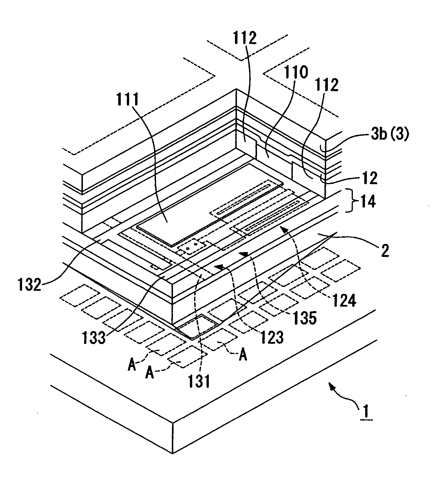
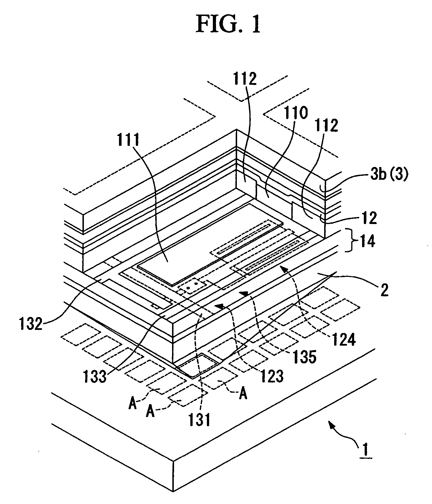
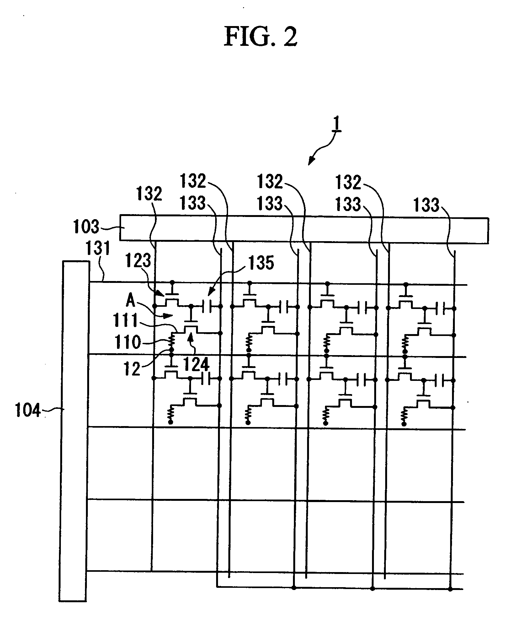
[0040]FIG. 1 is an explanatory diagram schematically illustrating the main parts of an organic electroluminescent (EL) device according to an embodiment of the invention, particularly, an active matrix organic EL device 1. In addition, the organic EL device 1 adopts an active matrix driving method using thin film transistors.

[0041] The organic EL device 1 is formed by laminating, on a substrate 2, a circuit element portion 14 including thin film transistors, serving as circuit elements, pixel electrodes (anodes) 111, a functional layer 110 including an organic EL layer (organic EL element), a cathode 12, a sealing portion 3, etc., in this order.

[0042] In this embodiment, a glass substrate is used as the substrate 2. However, various well-known substrates used for an electro-optical device or a circuit substrate, such as a silicon substrate, a quartz substrate, a ceramic substrate, a metal substrate, a plastic substrate, and a plastic film substrate, can be used as the substrate 2,...

second embodiment

[0080] Next, an organic EL device according to a second embodiment will be described with reference to FIG. 4. This embodiment is characterized in that the pixel electrodes 111 having a function of absorbing red light are provided in the green (G) and blue (B) pixels, unlike the first embodiment, and the other structures thereof are substantially the same as those in the first embodiment. Therefore, in this embodiment, components different from those in the first embodiment will be described in detail.

[0081] An organic EL device 100 of the second embodiment has the same structure as the organic EL device 1 of the first embodiment in the red (R) pixel. On the other hand, for the green (G) and blue (B) pixels, pixel electrodes 127 having both an electrode (anode) function and a filter function of absorbing light (corresponding to red light) having a wavelength greater than 550 nm are provided on the second interlayer insulating film 144b. More specifically, an Sn phthalocyanine compo...

third embodiment

[0084] Next, an organic EL device according to a third embodiment will be described with reference to FIG. 5. In the third embodiment, in the green (G) and blue (B) pixels, two pixel electrodes are formed in one pixel, and two TFTs are formed corresponding thereto, unlike the first and second embodiments. On the other hand, the red (R) pixel has the same structure as those in the first and second embodiments. Therefore, components different from those in the first and second embodiments will be described below in detail.

[0085] In an organic EL device 101 shown in FIG. 5, each of the green (G) and blue (B) pixels is divided into two dots, and two pixel electrodes are formed in one pixel. The two pixel electrodes formed in one pixel are a pixel electrode 127 (hereinafter, referred to as a colored pixel electrode 127), functioning as a red absorption filter, and the pixel electrode 111 not having the filter function, respectively, and the TFTs 123 are respectively connected to the pix...


PUM


Abstract

An organic EL device includes light-reflective electrodes; light-transmissive electrodes; organic EL layers that are respectively provided between the light-reflective electrodes and the light-transmissive electrodes to emit a plurality of color light components, the organic EL layer emitting a different color light component in each pixel; and transflective layers that are selectively provide in predetermined color pixels to reflect or transmit light emitted from the organic EL layers, respectively, each transflective layer being opposite to the light-reflective electrode with the organic EL layer interposed therebetween.

Description

CROSS-REFERENCE TO RELATED APPLICATIONS [0001] This application claims priority from Japanese Patent Application Nos. 2004-164493, filed on Jun. 2, 2004, and 2004-164495, filed on Jun. 2, 2004, the entire disclosures of which are incorporated herein by reference. BACKGROUND OF THE INVENTION [0002] 1. Technical Field [0003] The present invention relates to an organic EL device and to an electronic apparatus. [0004] 2. Related Art [0005] In recent years, organic electroluminescent (hereinafter, referred to as organic EL) devices in which a plurality of organic EL elements, serving as information display units, are provided in each pixel have been used in electronic apparatuses, such as notebook computers, cellular phones, and electronic organizers. In general, the organic EL element has a structure in which an organic functional layer including an organic EL layer (light-emitting layer) is interposed between a pair of electrodes. [0006] For example, Japanese Unexamined Patent Applicat...

Claims


Application Information

Patent Timeline
Patent Type & Authority Applications(United States)
IPC IPC(8): H01L27/32H01L51/52H05B33/00
CPCH01L27/3211H01L27/322H01L51/5265H01L27/3295H01L27/3244H10K59/35H10K59/38H10K59/122H10K59/12H10K50/852H05B33/24
Inventor KOBAYASHI, HIDEKAZU
Owner INTELLECTUAL KEYSTONE TECH LLC
Why Eureka
Try Eureka