Organic electroluminescent device and display device

An electroluminescent device and organic light-emitting layer technology, applied in organic light-emitting devices, organic light-emitting device parameters, electro-solid devices, etc., can solve the problems of wide spectrum, short device life, etc. Conducive to the narrowing effect of the spectrum

Active Publication Date: 2019-03-01
KUNSHAN GO VISIONOX OPTO ELECTRONICS CO LTD +1
View PDF5 Cites 78 Cited by
  • Summary
  • Abstract
  • Description
  • Claims
  • Application Information

AI Technical Summary

Problems solved by technology

[0004] The present invention provides an organic electroluminescent device and a display device. The organic light-emitting layer of the organic electroluminescent device uses a wide bandgap material as the main material, and uses TADF as a sensitizer material to assist sensitized resonance type TADF dyes to emit light, thereby Overcome the shortcomings of short device life and wide spectrum caused by the use of traditional TADF materials for light emission at this stage

Method used


Image

  • Organic electroluminescent device and display device
  • Organic electroluminescent device and display device
  • Organic electroluminescent device and display device

Examples


preparation example Construction

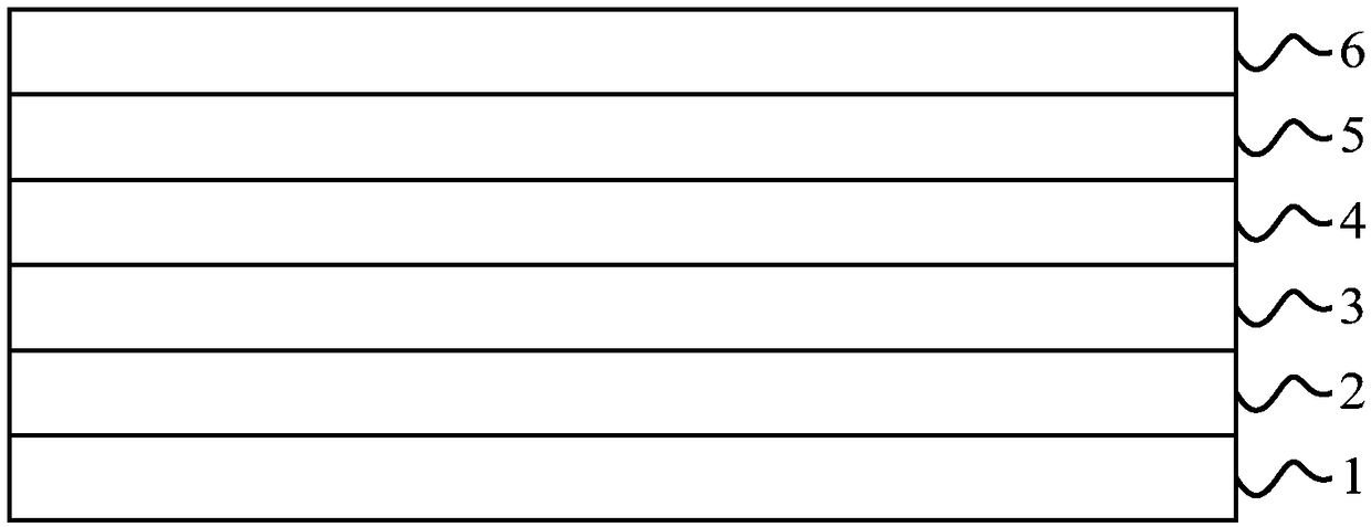
[0101] The present invention also provides a preparation method of the organic electroluminescent device, to figure 1 As an example, it includes sequentially depositing an anode 2 , a hole transport region 3 , an organic light-emitting layer 4 , an electron transport region 5 , and a cathode 6 on a substrate 1 , and then packaging. Wherein, when preparing the organic light-emitting layer 4, the organic light-emitting layer 4 is formed by co-evaporating the wide bandgap material source, the sensitizer material source and the resonant TADF material source.

[0102] Specifically, the preparation method of the organic electroluminescent device of the present invention comprises the following steps:

[0103] 1. Ultrasonically treat the glass plate coated with the anode material in a commercial cleaning agent, rinse in deionized water, ultrasonically degrease in acetone: ethanol mixed solvent, bake in a clean environment until the water is completely removed, and use ultraviolet lig...

Embodiment 1

[0112] The device structure of this embodiment is:

[0113] ITO / HI-2(10nm) / HT-27(40nm) / W-7:20wt%T-37:3wt%M-3(30nm) / ET-53(30nm) / LiF(0.5nm) / Al( 150nm)

[0114] Wherein, the anode is ITO; the material of the hole injection layer is HI-2, and the general total thickness is 5-30nm, which is 10nm in this embodiment; the material of the hole transport layer is HT-27, and the total thickness is generally 5-50nm, The present embodiment is 40nm; the host material of the organic light-emitting layer is wide bandgap material W-7, the sensitizer material is T-37 and the doping concentration is 20wt%, the dye is resonance type TADF material M-3 and the doping concentration is 3wt%, the thickness of the organic light-emitting layer is generally 1-60nm, and this embodiment is 30nm; the material of the electron transport layer is ET-53, and the thickness is generally 5-30nm, and this embodiment is 30nm; electron injection layer and cathode material selection LiF (0.5nm) and metallic aluminum...

Embodiment 2

[0117] The device structure of this embodiment is:

[0118] ITO / HI-2(10nm) / HT-27(40nm) / W-7:15wt%T-37:5wt%M-8(30nm) / ET-53(30nm) / LiF(0.5nm) / Al( 150nm)


PUM


Abstract

The invention provides an organic electroluminescent device and a display device. The organic electroluminescent device comprises an organic luminescent layer; the organic luminescent layer comprisesa main body material, a sensitizing agent material and a resonance thermally activated delayed fluorescence (TADF) material; the main body material is a broad-band gap material; the sensitizing agentmaterial is a thermally activated delayed fluorescence material; a singlet-state energy level of the thermally activated delayed fluorescence material is located between a singlet-state energy level of the broad-band gap material and a singlet-state energy level of the resonance thermally activated delayed fluorescence material; and a triplet-state energy level of the thermally activated delayed fluorescence material is located between a triplet-state energy level of the broad-band gap material and a triplet-state energy level of the resonance thermally activated delayed fluorescence material.With the organic electroluminescent device and the display device, the defects of short life time and wide spectrum of the device caused by a condition that the traditional TADF material is adopted to emit light at the present stage can be overcome.

Description

technical field [0001] The invention relates to an organic electroluminescence device and a display device, belonging to the technical field of organic electroluminescence. Background technique [0002] Organic Light Emitting Diode (OLED) is a device that is driven by current to achieve the purpose of emitting light. Its main characteristics come from the organic light-emitting layer. When an appropriate voltage is applied, electrons and holes Excitons are combined in the organic light-emitting layer to emit light of different wavelengths according to the characteristics of the organic light-emitting layer. At present, the light-emitting layer is composed of host materials and doped dyes, and the dyes are mostly selected from traditional fluorescent materials and traditional phosphorescent materials. Specifically, traditional fluorescent materials have the disadvantage of being unable to utilize triplet excitons. Although traditional phosphorescent materials can achieve 100...

Claims


Application Information

Patent Timeline
Patent Type & Authority Applications(China)
IPC IPC(8): H01L51/54H01L51/50
CPCH10K85/623H10K85/625H10K85/624H10K85/649H10K85/656H10K85/615H10K85/654H10K50/121H10K85/631H10K85/322H10K85/6574H10K85/6572H10K85/40H10K2101/00H10K2101/20
Inventor 段炼蔡明瀚宋晓增魏金贝
Owner KUNSHAN GO VISIONOX OPTO ELECTRONICS CO LTD
Why Eureka
Try Eureka