Light-Emitting Device and Electronic Device Using Light-Emitting Device

Active Publication Date: 2012-08-16
SEMICON ENERGY LAB CO LTD
View PDF7 Cites 80 Cited by
  • Summary
  • Abstract
  • Description
  • Claims
  • Application Information

AI Technical Summary

Benefits of technology

[0013]In view of the foregoing, one object of one embodiment of the present invention is to provide a light-emitting element in a light-emitting device, the light-emitting device, and an electronic device using the light-emitting device in which a light re

Problems solved by technology

With such a structure (bottom-emission structure) where light emitted from a light-emitting element is extracted to outside through a substrate provided with a transistor for controlling light emission or the like, there is a problem of low aperture ratio

Method used


Image

  • Light-Emitting Device and Electronic Device Using Light-Emitting Device
  • Light-Emitting Device and Electronic Device Using Light-Emitting Device
  • Light-Emitting Device and Electronic Device Using Light-Emitting Device

Examples


embodiment 1

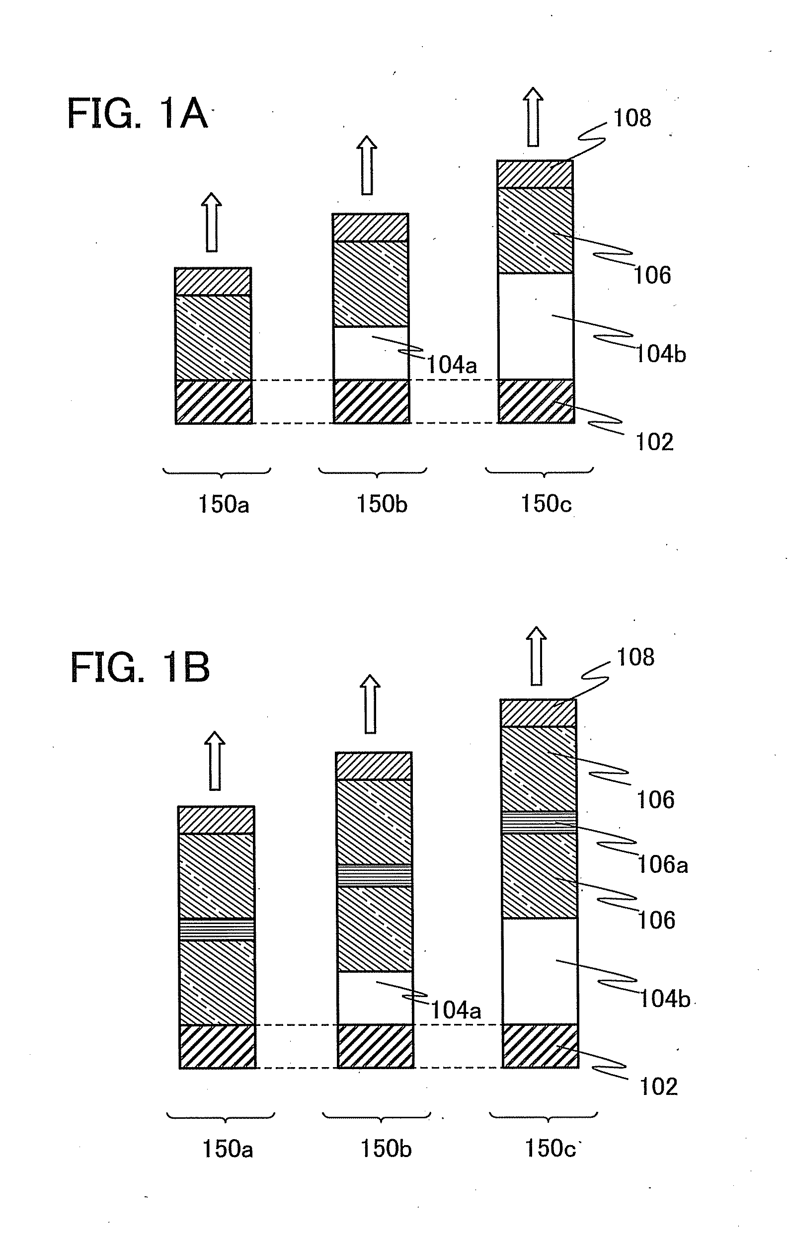
[0043]In Embodiment 1, one embodiment of a light-emitting device of the present invention is described using FIGS. 1A and 1B.

[0044]The light-emitting device shown in FIG. 1A is a cross-sectional diagram illustrating a concept of the present invention and includes a first light-emitting element 150a, a second light-emitting element 150b, and a third light-emitting element 150c. In the first light-emitting element 150a, a light-emitting layer 106 is provided in contact with a reflection electrode layer 102, and a transfiective electrode layer 108 is provided in contact with the light-emitting layer 106. In the second light-emitting element 150b, a first transparent electrode layer 104a is provided in contact with the reflection electrode layer 102, the light-emitting layer 106 is provided in contact with the first transparent electrode layer 104a, and the transflective electrode layer 108 is provided in contact with the light-emitting layer 106. In the third light-emitting element 150...

embodiment 2

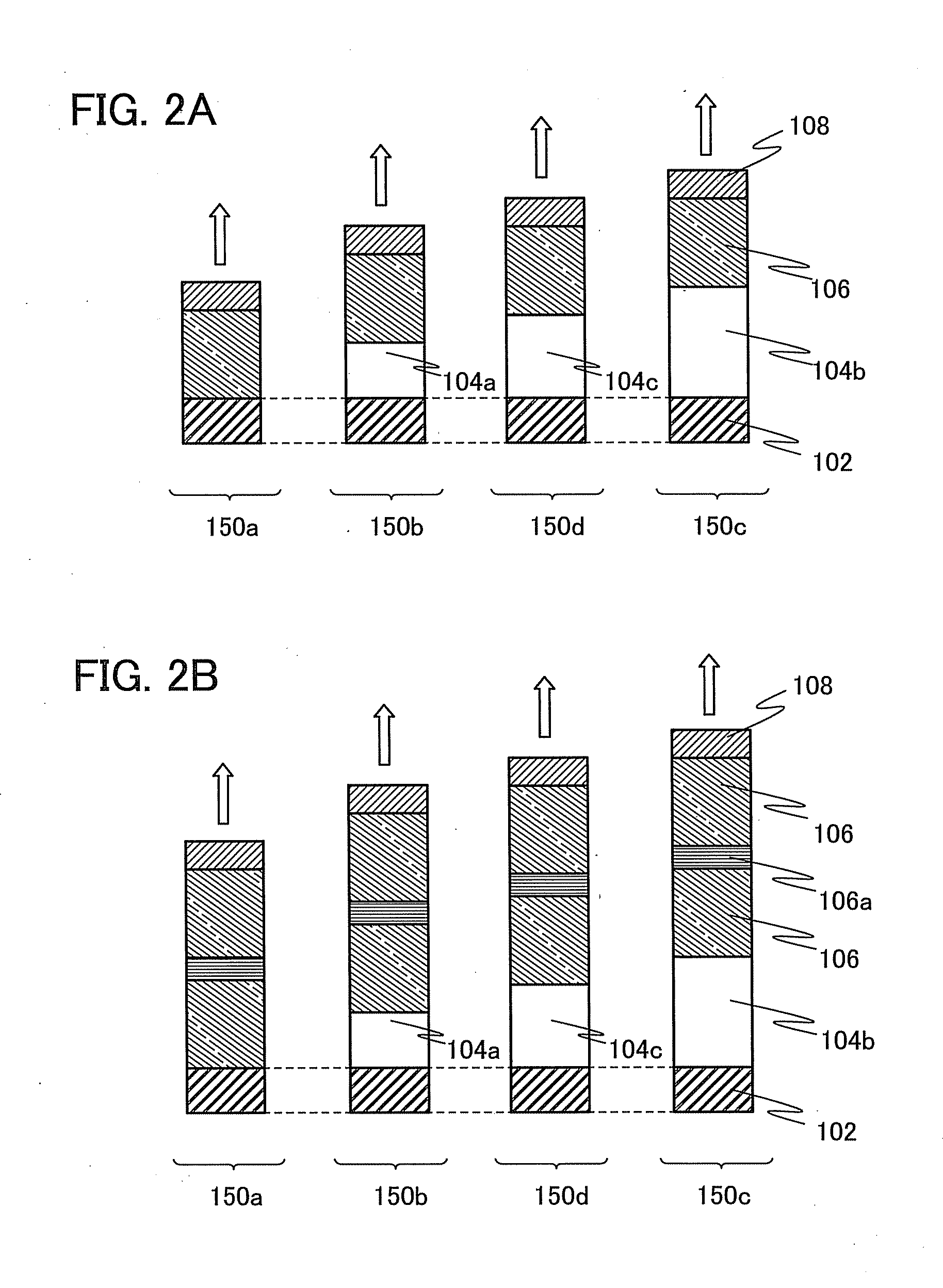
[0066]In this embodiment, structures of one embodiment of a light-emitting device of the present invention, which are different from Embodiment 1, are described using FIGS. 2A and 2B.

[0067]A light-emitting device shown in FIG. 2A is a cross-sectional diagram illustrating a concept of the present invention and includes a first light-emitting element 150a, a second light-emitting element 150b, a third light-emitting element 150c, and a fourth light-emitting element 150d. In the first light-emitting element 150a, a light-emitting layer 106 is provided in contact with a reflection electrode layer 102, and a transflective electrode layer 108 is provided in contact with the light-emitting layer 106. In the second light-emitting element 150b, a first transparent electrode layer 104a is provided in contact with the reflection electrode layer 102, the light-emitting layer 106 is provided in contact with the first transparent electrode layer 104a, and the transflective electrode layer 108 is ...

embodiment 3

[0081]In this embodiment, details about the light-emitting element including the refection electrode layer 102, the light-emitting layer 106, and the transflective electrode layer 108 described in Embodiment 1 and Embodiment 2 are described using FIGS. 3A and 3B.

[0082]A light-emitting element shown in FIG. 3A has a structure in which the light-emitting layer 106 including an emitting region is provided between a pair of electrodes (the refection electrode layer 102 and the transflective electrode layer 108). In this embodiment, the refection electrode layer 102 is used as an anode and the transflective electrode layer 108 is used as a cathode as an example.

[0083]The light-emitting layer 106 includes at least a light-emitting layer and may include any functional layer in addition to the light-emitting layer. Examples of the functional layer other than the light-emitting layer include a layer containing a substance having high hole-injection properties, a substance having high hole-tr...


PUM


Abstract

First to third light-emitting elements each including a reflection electrode layer, a transflective electrode layer, and a light-emitting layer provided therebetween are provided. In the first light-emitting element, the light-emitting layer is in contact with the reflection electrode layer and the transflective electrode layer. In the second light-emitting element, a first transparent electrode layer is in contact with the reflection electrode layer, the light-emitting layer is in contact with the first transparent electrode layer and the transflective electrode layer. In the third light-emitting element, a second transparent electrode layer is in contact with the reflection electrode layer, the light-emitting layer is in contact with the second transparent electrode layer and the transflective electrode layer. The first transparent electrode layer is different form the second transparent electrode layer in thickness.

Description

BACKGROUND OF THE INVENTION[0001]1. Field of the Invention[0002]One embodiment of the present invention relates to a light-emitting device using electroluminescence. Further, one embodiment of the present invention relates to an electronic device using the light-emitting device.[0003]2. Description of the Related Art[0004]In recent years, research and development have been actively conducted on light-emitting elements using electroluminescence (EL). In a basic structure of such a light-emitting element, a layer containing a substance with a light-emitting property is provided between a pair of electrodes. A voltage is applied to this element, so that light emission from the light-emitting substance can be obtained.[0005]Since the above light-emitting element is a self-luminous type, and thus a light-emitting device using the light-emitting element has advantages such as high visibility, no necessity of a backlight, and low power consumption. In addition, such a light-emitting device...

Claims


Application Information

Patent Timeline
IPC IPC(8): G02F1/1335H01L33/08
CPCH01L27/1225H01L27/3211H01L27/322H05B33/22H01L27/3244H01L51/5265H01L27/3232H10K59/50H10K59/35H10K59/38H10K59/12H10K50/852H01L31/022466H01L2924/01042H10K59/122H10K50/17
Inventor SEO, SATOSHISASAKI, TOSHIKIOHSAWA, NOBUHARU
Owner SEMICON ENERGY LAB CO LTD
Why Eureka
Try Eureka