Semiconductor device and a manufacturing method thereof

a technology of semiconductor devices and manufacturing methods, applied in semiconductor devices, semiconductor/solid-state device details, electrical apparatus, etc., can solve problems such as delay due to complicated wiring, increase in the number of elements that should be integrated, so as to improve the reliability of super-miniaturized and high-speed semiconductor devices. , the effect of large resistance to electro migration

Inactive Publication Date: 2007-10-09
FUJITSU LTD
View PDF17 Cites 5 Cited by
  • Summary
  • Abstract
  • Description
  • Claims
  • Application Information

AI Technical Summary

Benefits of technology

[0023]According to the present invention, reliability of a super-miniaturized and high-speed semiconductor device can be greatly enhanced by forming a middle layer of a high melting-point metal, such as tungsten (W), that has a large resistance against the electro migration, inside of the via hole where current concentration tends to grow in the Cu multilayer interconnection structure, in thickness that is sufficient to perform as a barrier against the electro migration, and that does not cause effective electric resistance to increase, in only a part in a depth direction of the via hole. According to the present invention, the middle layer of the high melting-point metal can be formed in a self-alignment manner, avoiding an increase in the number of mask processes.

Problems solved by technology

The number of elements that should be integrated is increasing, and wiring is becoming complicated by the large scale integration.
In the multilayer interconnection, however, delay due to complicated wiring is a concern, and Cu wiring is attracting attention because of a low resistance value, especially in wiring of logic LSIs.
However, local current concentration still arises to a via plug in the Cu wiring laminated structure that is miniaturized, causing a poor wiring by a void generated as explained above.

Method used


Image

  • Semiconductor device and a manufacturing method thereof
  • Semiconductor device and a manufacturing method thereof
  • Semiconductor device and a manufacturing method thereof

Examples


Embodiment Construction

[0033]In the following, embodiments of the present invention will be described with reference to the accompanying drawings.

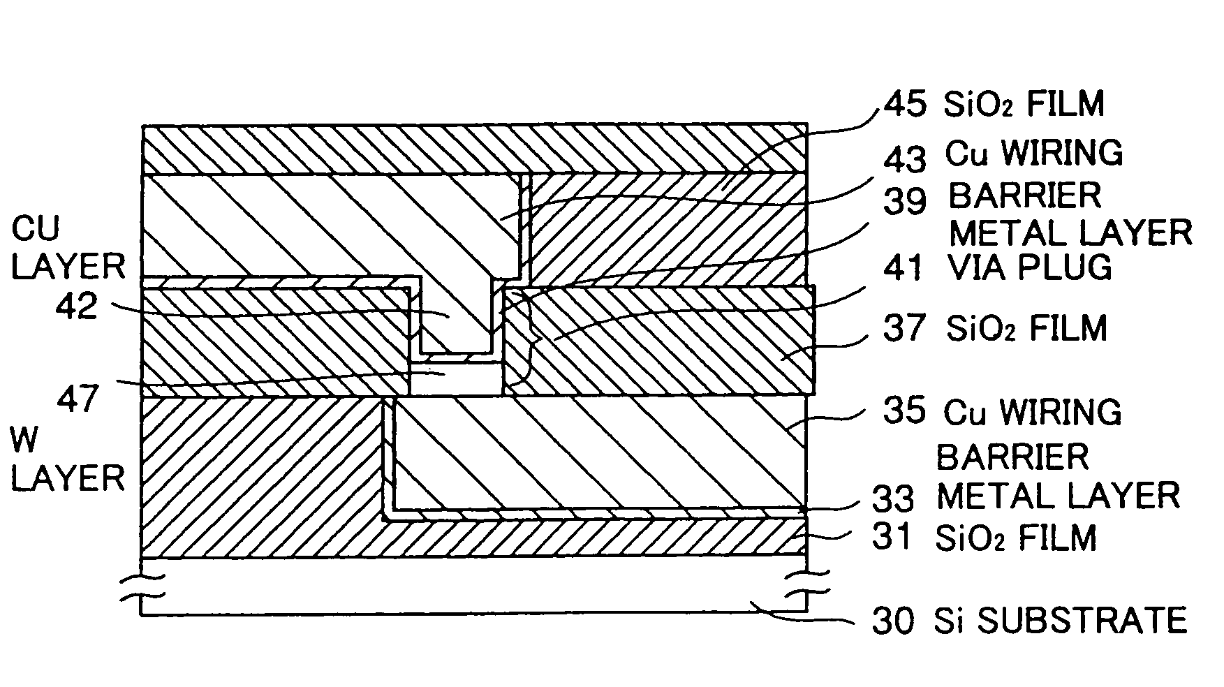
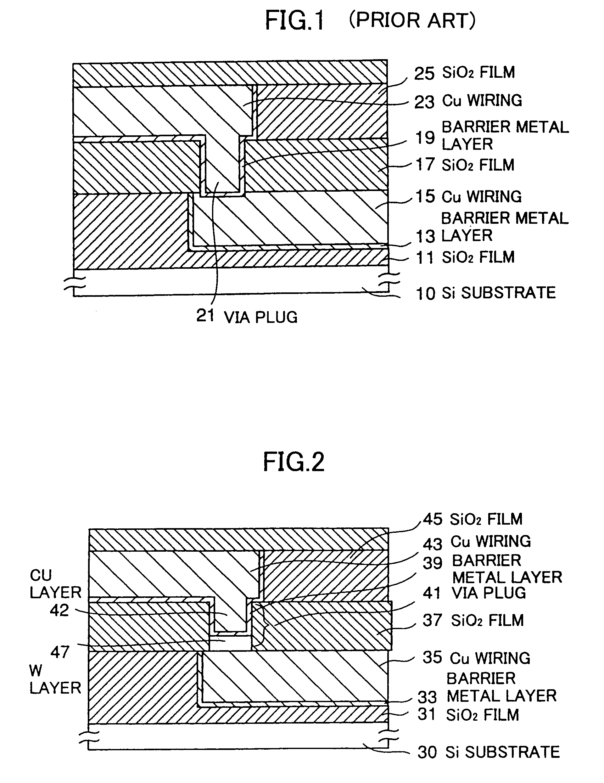
[0034]FIG. 2 is a figure explaining wiring structure of the semiconductor device of the embodiments of the present invention.

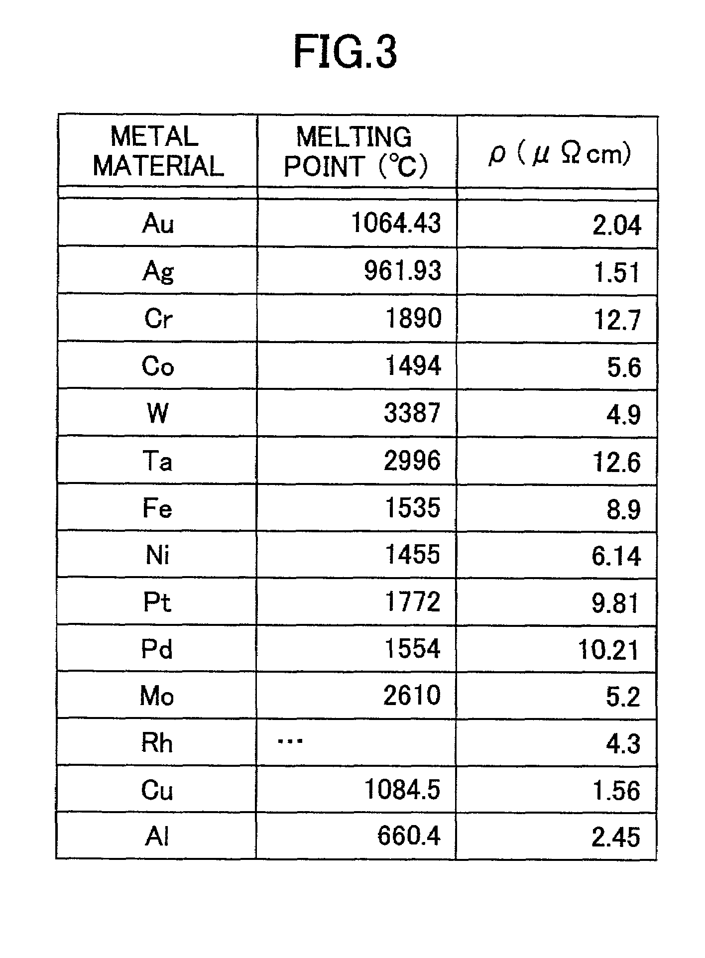
[0035]The semiconductor device of the embodiment has multilayer interconnection structure that employs Cu wiring 35 and Cu wiring 43. In a via plug 41, a Cu layer 42 formed contiguously with the Cu wiring 43, and a W layer 47 as a high melting-point metal layer are included. The metal material adopted as this high melting-point metal layer is chosen with reference to the melting point and the specific resistance of Cu that forms the Cu wiring 35, the Cu wiring 43, and the Cu layer 42, and is formed in predetermined thickness.

[0036]With reference to FIG. 2, the wiring structure of the semiconductor device of the embodiment is explained. First, on a semiconductor (Si) substrate 30, a silicon dioxide (SiO2) film 31 as an inter-layer film to w...


PUM

PropertyMeasurementUnit
thicknessaaaaaaaaaa
thicknessaaaaaaaaaa
thicknessaaaaaaaaaa

Abstract

A multilayer interconnection structure that offers a fast semiconductor operation is realized by employing copper wiring, electro migration of which is prevented from occurring by providing a via plug that includes a layer of a high melting-point metal, such as tungsten.

Description

BACKGROUND OF THE INVENTION[0001]1. Field of the Invention[0002]The present invention generally relates to a semiconductor device and a manufacturing method thereof, and particularly relates to the semiconductor device that has multilayer interconnection structure, and the manufacturing method thereof.[0003]2. Description of the Related Art[0004]Miniaturization of wiring design rule of semiconductor devices is progressing with rapid development of ULSI (Ultra Large Scale Integration) technology. The number of elements that should be integrated is increasing, and wiring is becoming complicated by the large scale integration. Multilayer interconnection attracts attention in order to cope with this situation.[0005]In the multilayer interconnection, however, delay due to complicated wiring is a concern, and Cu wiring is attracting attention because of a low resistance value, especially in wiring of logic LSIs.[0006]FIG. 1 is a figure explaining wiring structure of a conventional semicon...

Claims


Application Information

Patent Timeline
Patent Type & Authority Patents(United States)
IPC IPC(8): H01L23/48H01L21/3205H01L21/768H01L23/522H01L23/532
CPCH01L21/76843H01L21/76847H01L21/76849H01L21/7685H01L21/76877H01L21/76879H01L23/5226H01L23/53238H01L23/53257H01L2924/0002H01L2924/00H01L21/3205
Inventor KITADA, HIDEKISHIMIZU, NORIYOSHIOHTSUKA, NOBUYUKIOHBA, TAKAYUKI
Owner FUJITSU LTD
Why Eureka
Try Eureka