Semiconductor device and display device including the semiconductor device

Inactive Publication Date: 2017-09-21
SEMICON ENERGY LAB CO LTD
View PDF1 Cites 10 Cited by
  • Summary
  • Abstract
  • Description
  • Claims
  • Application Information

AI Technical Summary

Benefits of technology

[0009]The layout area of transistors can be reduced by stacking a plurality of transistors as disclosed in Patent Documents 1 and 2. On t

Problems solved by technology

On the other hand, there is a problem in that the stacking of a plurali

Method used


Image

  • Semiconductor device and display device including the semiconductor device
  • Semiconductor device and display device including the semiconductor device
  • Semiconductor device and display device including the semiconductor device

Examples


embodiment 1

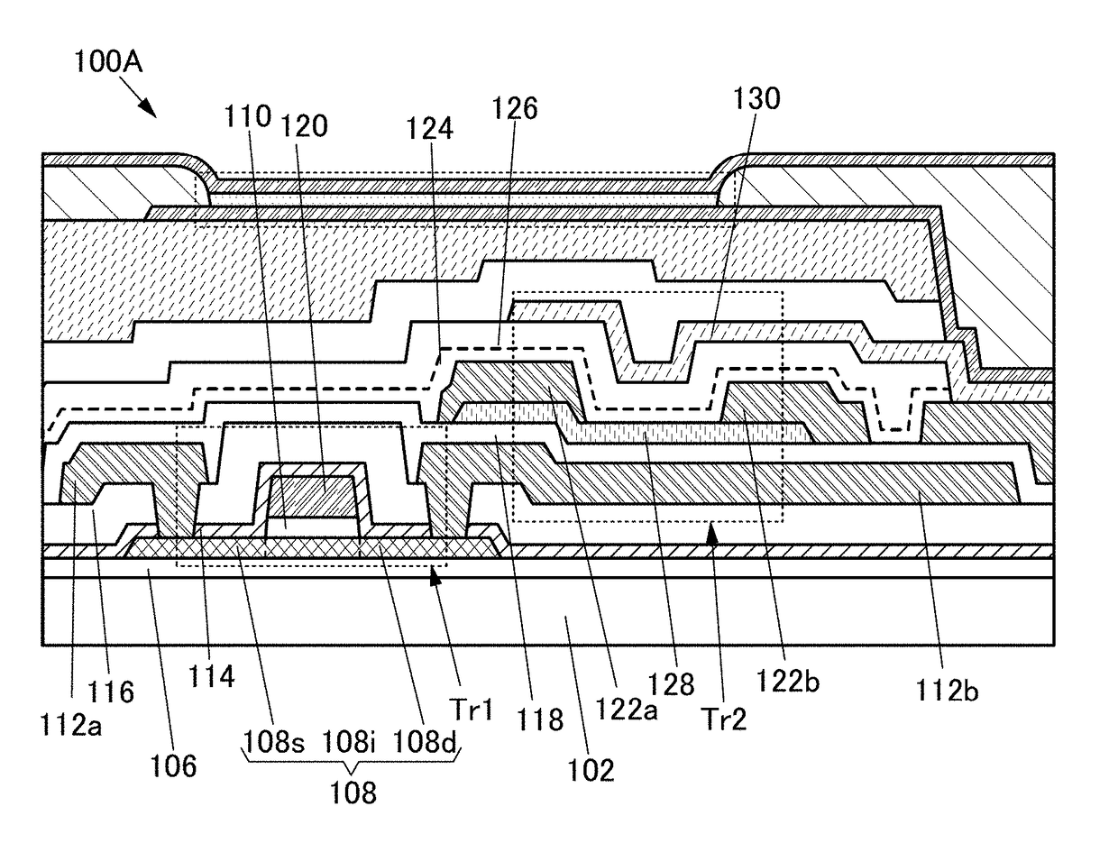
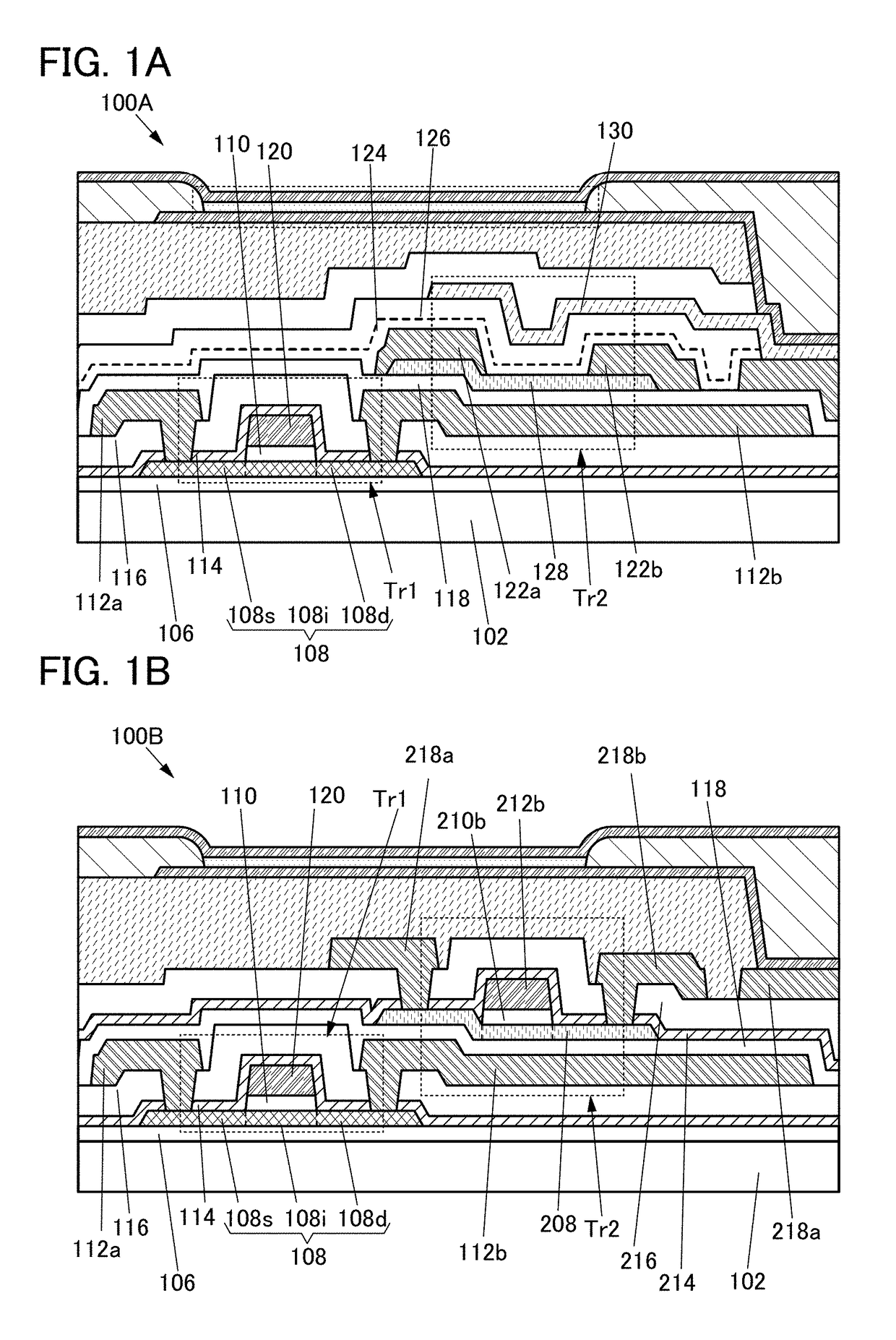
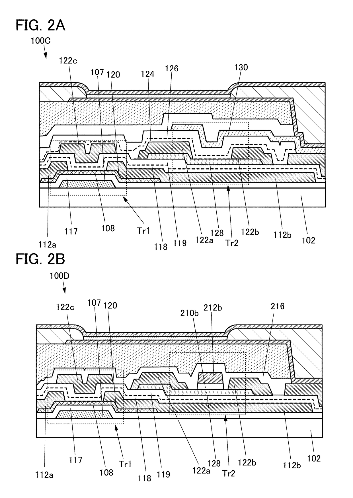
[0111]In this embodiment, a semiconductor device that is one embodiment of the present invention and a method of manufacturing the semiconductor device are described with reference to FIGS. 1A and 1B, FIGS. 2A and 2B, FIGS. 3A and 3B, FIGS. 4A and 4B, FIGS. 5A and 5B, FIG. 6, FIG. 7, FIGS. 8A to 8C, FIG. 9, FIG. 10, FIG. 11, FIGS. 12A and 12B, FIGS. 13A and 13B, FIGS. 14A and 14B, FIGS. 15A and 15B, FIGS. 16A and 16B, FIGS. 17A and 17B, FIGS. 18A and 18B, FIGS. 19A and 19B, FIGS. 20A and 20B, FIGS. 21A and 21B, FIGS. 22A and 22B, and FIGS. 23A and 23B.

[0112]Cross-sectional views of semiconductor devices 100A, 100B, 100C, and 100D of one embodiment of the present invention are shown (see FIGS. 1A and 1B and FIGS. 2A and 2B). The semiconductor devices 100A, 100B, 100C, and 100D each include a transistor Tr1 and a transistor Tr2.

[0113]The transistor Tr1 and the transistor Tr2 of the semiconductor device 100A are a top-gate transistor and a bottom-gate transistor, respectively. The tran...

embodiment 2

[0394]The composition of an oxide semiconductor film relating to the present invention is described below.

[0395]An oxide preferably contains at least indium or zinc. In particular, indium and zinc are preferably contained. In addition, aluminum, gallium, yttrium, tin, or the like is preferably contained. Furthermore, one or more elements selected from boron, silicon, titanium, iron, nickel, germanium, zirconium, molybdenum, lanthanum, cerium, neodymium, hafnium, tantalum, tungsten, magnesium, and the like may be contained.

[0396]Here, the case where an oxide contains indium, an element M, and zinc is considered. The element M is aluminum, gallium, yttrium, tin, or the like. Alternatively, the element M can be boron, silicon, titanium, iron, nickel, germanium, zirconium, molybdenum, lanthanum, cerium, neodymium, hafnium, tantalum, tungsten, magnesium, or the like. Note that two or more of the above elements may be used in combination as the element M in some cases.

[0397]First, preferr...

embodiment 3

[0565]In this embodiment, a semiconductor device and a method of manufacturing the semiconductor device of one embodiment of the present invention are described with reference to FIGS. 40A and 40B, FIGS. 41A and 41B, FIGS. 42A and 42B, FIGS. 43A and 43B, FIGS. 44A and 44B, FIGS. 45A and 45B, FIGS. 46A and 46B, and FIGS. 47A and 47B.

[0566]FIG. 40A is a top view of a semiconductor device 200 of one embodiment of the present invention. FIG. 40B is a cross-sectional view taken along dashed dotted line A1-A2 in FIG. 40A. Note that cross sections in a channel length (L) direction of the transistor Tr1 and in a channel length (L) direction of the transistor Tr2 are included in FIG. 40B.

[0567]The semiconductor device 200 illustrated in FIGS. 40A and 40B includes the transistor Tr1 and the transistor Tr2 which overlaps at least partly with the transistor Tr1. Note that the transistor Tr1 and the transistor Tr2 are top-gate transistors.

[0568]Since the transistor Tr1 overlaps at least partly w...


PUM


Abstract

A semiconductor device with a reduced layout area of transistors is provided. The semiconductor device includes a first transistor including a first oxide semiconductor film and a second transistor including a second oxide semiconductor film over a substrate. When the oxide semiconductor films are subjected to electron diffraction, the ratio of the integrated intensity of luminance of a diffraction spot derived from c-axis alignment to the integrated intensity of luminance of a diffraction spot derived from alignment in any direction in the first oxide semiconductor film is higher than that in the second oxide semiconductor film. In addition, part of the first transistor is located between the second transistor and the substrate.

Description

BACKGROUND OF THE INVENTION[0001]1. Field of the Invention[0002]One embodiment of the present invention relates to a semiconductor device including an oxide semiconductor film and a display device including the semiconductor device.[0003]Note that one embodiment of the present invention is not limited to the above technical field. The technical field of one embodiment of the invention disclosed in this specification and the like relates to an object, a method, or a manufacturing method. The present invention relates to a process, a machine, manufacture, or a composition of matter. In particular, one embodiment of the present invention relates to a semiconductor device, a display device, a light-emitting device, a power storage device, a storage device, a driving method thereof, and a manufacturing method thereof.[0004]In this specification and the like, a semiconductor device generally means a device that can function by utilizing semiconductor characteristics. A semiconductor eleme...

Claims


Application Information

Patent Timeline
IPC IPC(8): H01L27/12H01L29/04H01L29/24H01L29/786
CPCH01L27/1229H01L27/1225H01L29/7869H01L29/78696H01L27/1222H01L29/24H01L27/3262H01L29/786H01L29/045H01L29/78648H01L27/1251H10K59/1213
Inventor YAMAZAKI, SHUNPEIOKAZAKI, KENICHIMIYAKE, HIROYUKIAKIMOTO, KENGOJINTYOU, MASAMIIGUCHI, TAKAHIRO
Owner SEMICON ENERGY LAB CO LTD
Why Eureka
Try Eureka