Semiconductor device and display device including the semiconductor device

Active Publication Date: 2017-06-29
SEMICON ENERGY LAB CO LTD
View PDF0 Cites 20 Cited by
  • Summary
  • Abstract
  • Description
  • Claims
  • Application Information

AI Technical Summary

Benefits of technology

[0007]The transistor area can be reduced by stacking a plurality of transistors as disclosed in Patent Documents 1 and 2. On the other han

Problems solved by technology

On the other hand, there is a problem in that the stacking of a plurality of

Method used


Image

  • Semiconductor device and display device including the semiconductor device
  • Semiconductor device and display device including the semiconductor device
  • Semiconductor device and display device including the semiconductor device

Examples


embodiment 1

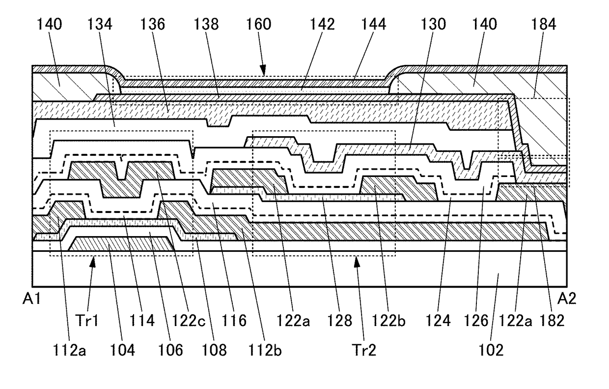
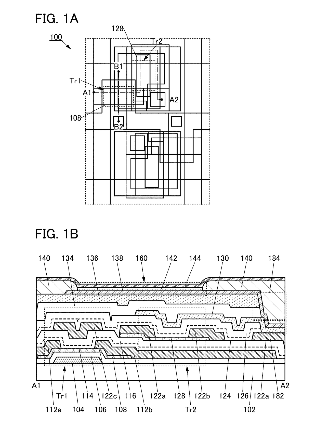
[0119]In this embodiment, a semiconductor device that is one embodiment of the present invention and a method of manufacturing the semiconductor device are described with reference to FIGS. 1A and 1B to FIGS. 17A and 17B.

1-1. Structure Example 1 of Semiconductor Device

[0120]FIG. 1A is a top view of a semiconductor device 100 of one embodiment of the present invention. FIG. 1B is a cross-sectional view taken along dashed dotted line A1-A2 in FIG. 1A. Note that cross sections in a channel length (L) direction of a transistor Tr1 and in a channel length (L) direction of a transistor Tr2 are included in FIG. 1B.

[0121]Note that some components (e.g., an insulating film serving as a gate insulating film) of the semiconductor device 100 and some reference numerals of components are not illustrated in FIG. 1A to avoid complexity. Note that some components and some reference numerals of components are not illustrated as in FIG. 1A in some cases in top views of semiconductor devices described...

embodiment 2

[0293]In this embodiment, a semiconductor device a method of manufacturing the semiconductor device of one embodiment of the present invention are described with reference to FIGS. 18A and 18B to FIGS. 29A and 29B

2-1. Structure Example 1 of Semiconductor Device

[0294]FIG. 18A is a top view of a semiconductor device 200 of one embodiment of the present invention. FIG. 18B is a cross-sectional view taken along dashed dotted line A1-A2 in FIG. 18A. Note that cross sections in a channel length (L) direction of the transistor Tr1 and in a channel length (L) direction of the transistor Tr2 are included in FIG. 18B.

[0295]The semiconductor device 100 illustrated in FIGS. 18A and 18B includes the transistor Tr1 and the transistor Tr2 which overlaps at least partly with the transistor Tr1. Note that the transistor Tr1 and the transistor Tr2 are a bottom-gate transistor and a top-gate transistor, respectively.

[0296]Since the transistor Tr1 overlaps at least partly with the transistor Tr2, the t...

embodiment 3

[0351]In this embodiment, a semiconductor device that is one embodiment of the present invention and a method of manufacturing the semiconductor device are described with reference to FIGS. 30A and 30B to FIGS. 45A and 45B.

3-1. Structure Example 1 of Semiconductor Device

[0352]FIG. 30A is a top view of a semiconductor device 300 of one embodiment of the present invention. FIG. 30B is a cross-sectional view taken along dashed dotted line A1-A2 in FIG. 30A. Note that cross sections in a channel length (L) direction of a transistor Tr1 and in a channel length (L) direction of a transistor Tr2 are included in FIG. 30B.

[0353]Note that some components (e.g., an insulating film serving as a gate insulating film) of the semiconductor device 100 and some reference numerals of components are not illustrated in FIG. 30A to avoid complexity. Note that some components and some reference numerals of components are not illustrated as in FIG. 30A in some cases in top views of semiconductor devices d...


PUM


Abstract

Provided is a novel semiconductor device. The semiconductor device comprises a first transistor and a second transistor. The first transistor comprises a first gate electrode; a first insulating film over the first gate electrode; a first oxide semiconductor film over the first insulating film; a first source electrode and a first drain electrode over the first oxide semiconductor film; a second insulating film over the first oxide semiconductor film, the first source electrode, and the first drain electrode; and a second gate electrode over the second insulating film. The second transistor comprises a first drain electrode; the second insulating film over the second drain electrode; a second oxide semiconductor film over the second insulating film; a second source electrode and a second drain electrode over the second oxide semiconductor film; a third insulating film over the second oxide semiconductor film, the second source electrode, and the second drain electrode; and a third gate electrode over the third insulating film. The first oxide semiconductor film partly overlaps with the second oxide semiconductor film.

Description

TECHNICAL FIELD[0001]One embodiment of the present invention relates to a semiconductor device including an oxide semiconductor film and a display device including the semiconductor device.[0002]Note that one embodiment of the present invention is not limited to the above technical field. The technical field of one embodiment of the present invention disclosed in this specification and the like relates to an object, a method, or a manufacturing method. The present invention relates to a process, a machine, manufacture, or a composition of matter. In particular, one embodiment of the present invention relates to a semiconductor device, a display device, a light-emitting device, a power storage device, a storage device, a driving method thereof, and a manufacturing method thereof.[0003]In this specification and the like, a semiconductor device generally means a device that can function by utilizing semiconductor characteristics. A semiconductor element such as a transistor, a semicond...

Claims


Application Information

Patent Timeline
IPC IPC(8): H01L27/12H01L51/00H01L29/04H01L29/66H01L29/786H01L29/24
CPCH01L27/1225H01L29/7869H01L29/78696H01L29/78648H01L29/78606H01L27/3262H01L29/045H01L29/66969H01L27/127H01L51/005H01L29/24H01L27/1255H10K59/12H01L29/7782H01L29/7786H10K59/1213H10K85/60
Inventor MIYAKE, HIROYUKIOKAZAKI, KENICHIHOSAKA, YASUHARUSHIMA, YUKINORI
Owner SEMICON ENERGY LAB CO LTD
Why Eureka
Try Eureka