

Fabrication method of vertical silicon nanowire field effect transistor
a technology of vertical silicon nanowires and field effect transistors, which is applied in the direction of nanotechnology, electrical equipment, semiconductor devices, etc., can solve the problems of achieving the the speed and performance of the transistor may be adversely affected, and the limitation of the conventional vertical silicon nanowire field effect transistor, etc., to reduce leakage current, suppress the short channel effect, and improve the effect of gate control ability
- Summary
- Abstract
- Description
- Claims
- Application Information
AI Technical Summary
Benefits of technology
Problems solved by technology
Method used
Image

Examples
Embodiment Construction
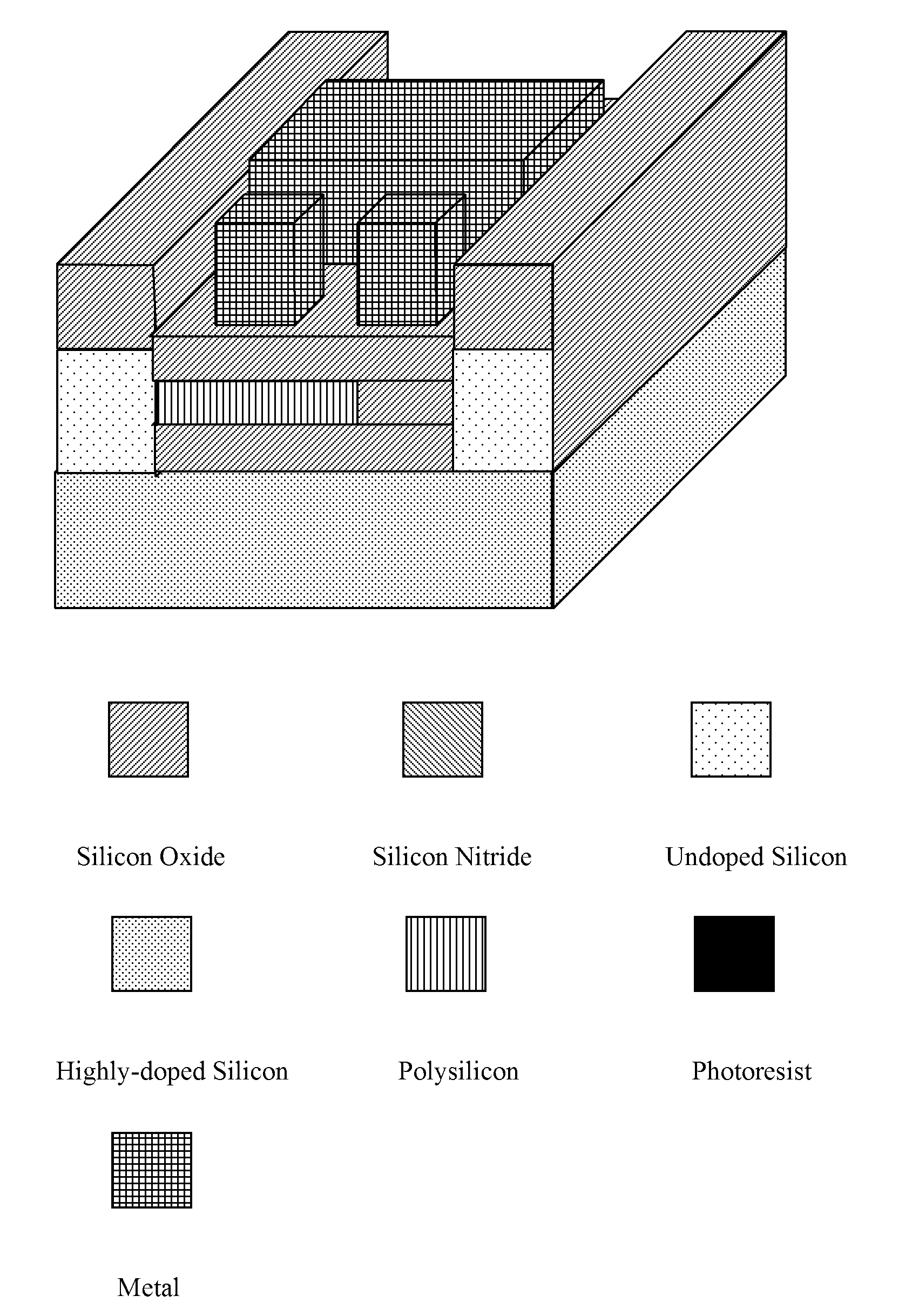
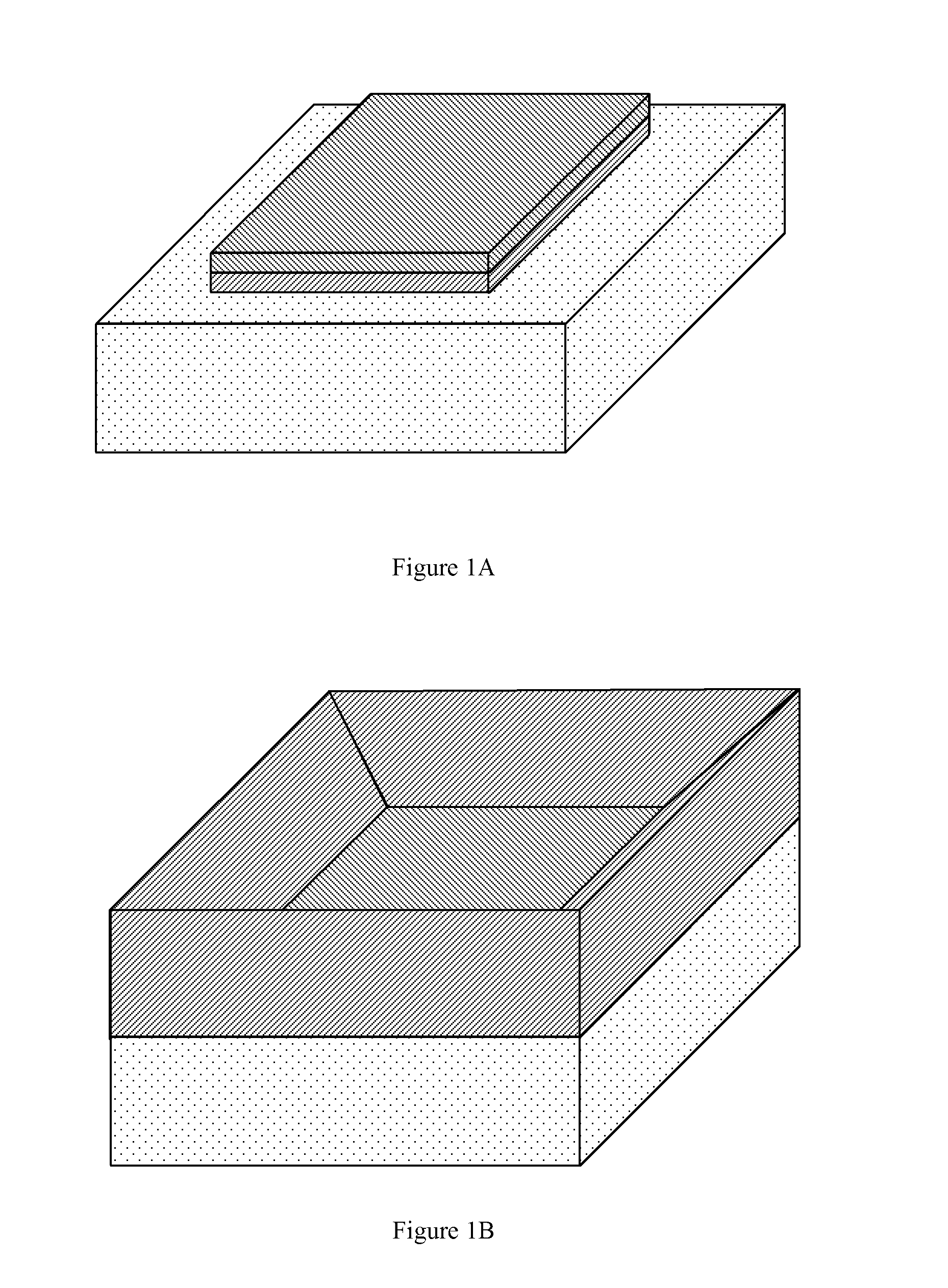
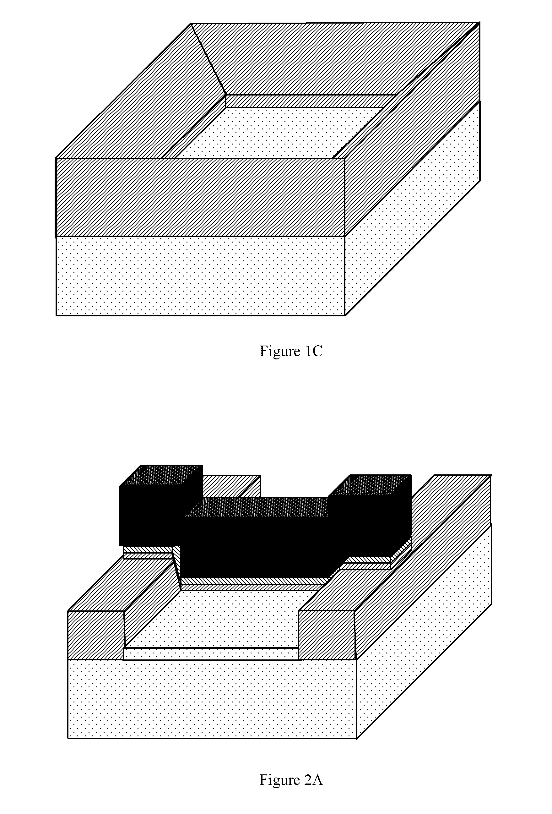
[0108]Hereinafter, an embodiment of the present invention will be described in more detail with reference to drawings and a specific embodiment. Herein, it is provided a solution for a process of a vertical silicon nanowire field effect transistor having a low parasitic resistance according to an embodiment of the present invention. However, the description does not limit the scope of the present invention by any way.
[0109]The vertical silicon nanowire field effect transistor having a channel length of about 90 nm and a diameter of about 10 nm is fabricated by the following steps.
[0110]1. A silicon oxide of 300 Å is deposited by using a low pressure chemical vapor deposition process.
[0111]2. A silicon nitride of 1000 Å is deposited by using a low pressure chemical vapor deposition process.
[0112]3. A photolithography process is performed to define an active region.
[0113]4. The silicon nitride of 1000 Å is etched by using an anisotropic dry etching process.
[0114]5. The silicon oxide o...
PUM
 Abstract
Description
Claims
Application Information