

Vertical PMOS field effect transistor and manufacturing method thereof
a technology of pmos field and transistor, which is applied in the direction of basic electric elements, electrical equipment, semiconductor devices, etc., can solve the problems of inability to enhance the performance of the transistor, difficulty in etc., and achieve the effects of reducing the lateral unit area of the transistor, increasing the element density of the semiconductor, and increasing the transport speed of the transistor carrier
- Summary
- Abstract
- Description
- Claims
- Application Information
AI Technical Summary
Benefits of technology
Problems solved by technology
Method used
Image

Examples
Embodiment Construction
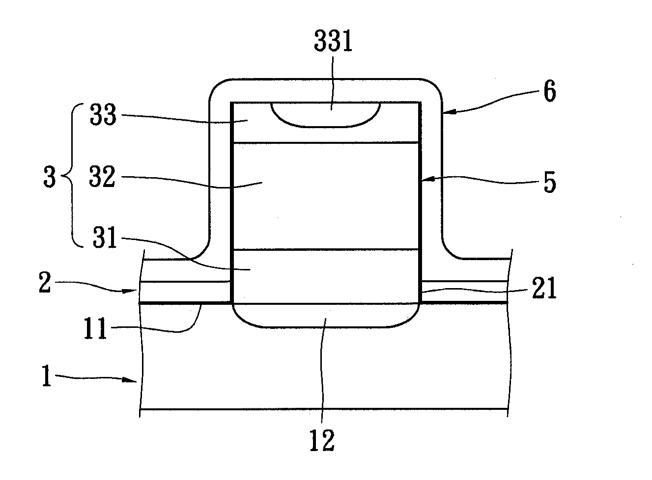
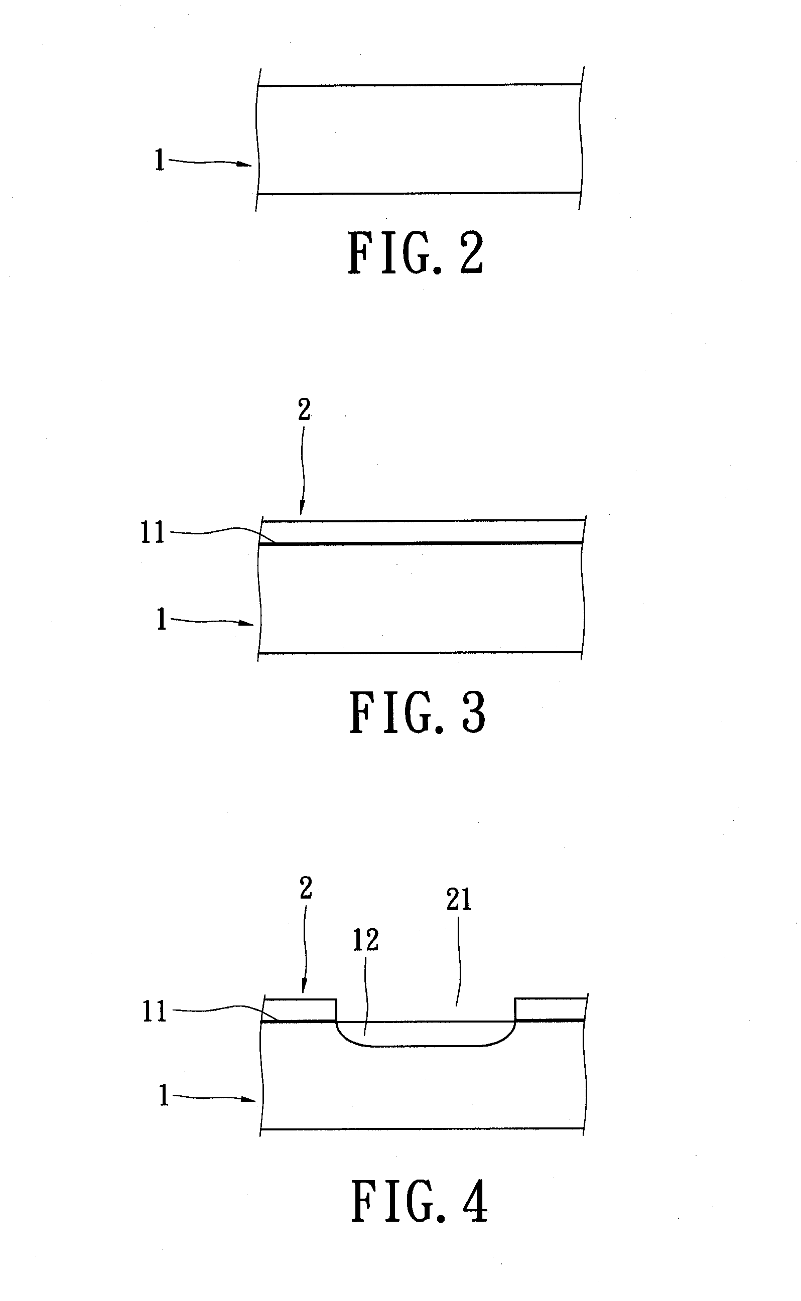
[0034]Reference is made to FIGS. 2˜11, which show the steps of the manufacturing method for a PMOS field effect transistor of the present invention. The manufacturing method for a PMOS field effect transistor of the present invention can be applied to the transistor for a DRAM. Reference is made to FIG. 2, which shows the step 1. A N-type Si substrate 1 is provided, which N-type means phosphorus doped wafer.
[0035]Reference is made to FIG. 3, which shows the step 2. A substrate oxide layer 11 is formed on the substrate 1 by thermal oxidation method. A first nitride layer 2 is deposited on the substrate oxide layer 11. The first nitride layer 2 is a isolation layer. In this embodiment, the first nitride layer 2 is composed of nitride silicon. In other embodiment, the first nitride layer 2 also can be composed of phosphorous silicon glass or boron phosphorous silicon glass.
[0036]Reference is made to FIG. 4, which shows the step 3. A pattern of a substrate concave trough 21 is defined o...
PUM
 Abstract
Description
Claims
Application Information