Mosfet and manufacturing method thereof

a technology of mosfet and manufacturing method, which is applied in the field of mosfet, can solve the problems of increased offleak current at drain junction, difficulty in balancing, and harmful effects of mosfet saturation current reduction, and achieve the effect of improving the basic performance of a transistor and high levels

Inactive Publication Date: 2009-10-22
LAPIS SEMICON CO LTD
View PDF10 Cites 2 Cited by
  • Summary
  • Abstract
  • Description
  • Claims
  • Application Information

AI Technical Summary

Benefits of technology

[0005]The present invention has been made in terms of the foregoing. It is therefore an object of the present invention to provide a MOSFET capable of improving the basic performance of a transistor such as saturation current characteristics, input follow-up and an offleak current at high levels, and a manufacturing method thereof.

Problems solved by technology

However, the high-concentration doping to the channel region yields a reduction in the mobility of carriers, thus resulting in the harmful effects of the saturation current of the MOSFET being reduced.
When, however, the relatively high-concentration layer is formed at the drain region end, an increase in the offleak current at a drain junction is incurred.
However, all the measures for performing improvements in saturation current characteristics cause even an increase in the offleak current, thus encountering difficulties in balancing these with each other at high levels.

Method used


Image

  • Mosfet and manufacturing method thereof
  • Mosfet and manufacturing method thereof

Examples


Embodiment Construction

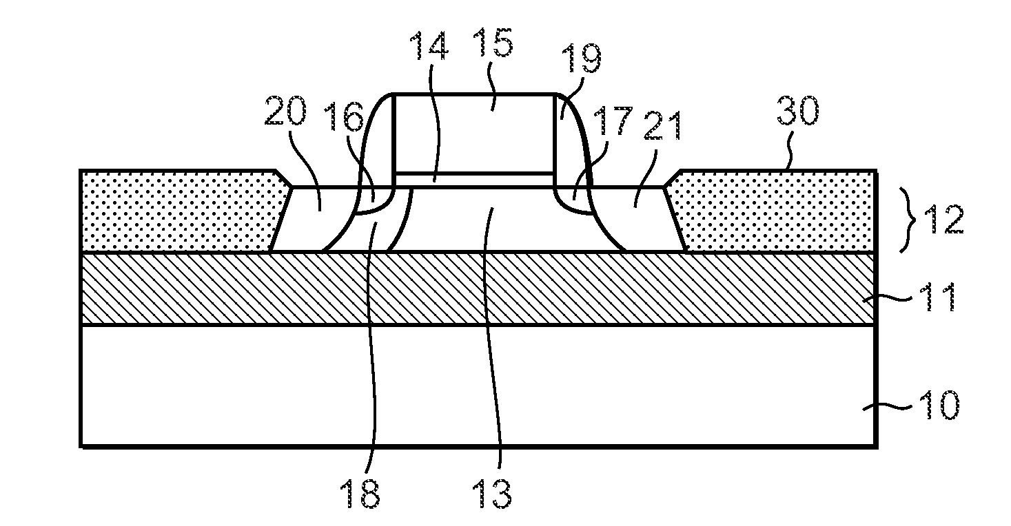
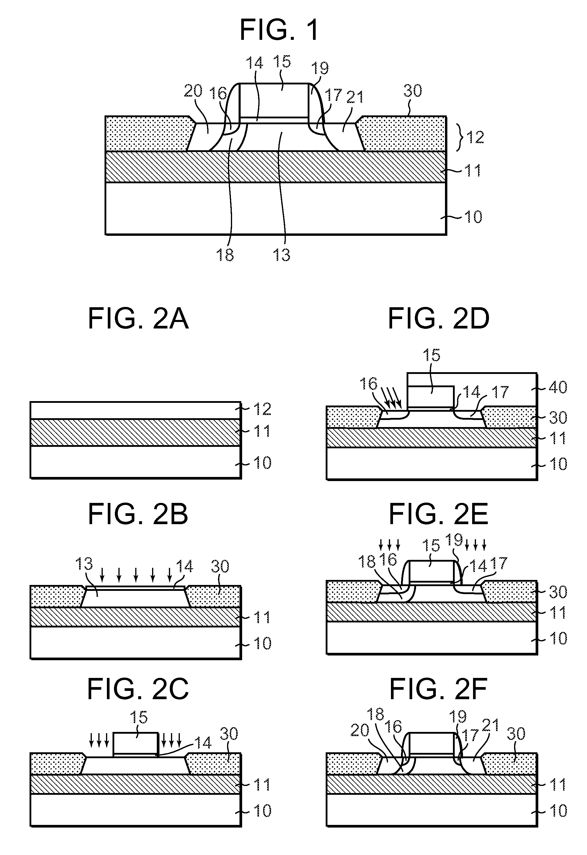
[0011]Preferred embodiments of the present invention will hereinafter be described with reference to the accompanying drawings. In the drawings shown below, the same reference numerals are respectively attached to components or parts substantially identical or equal to one another. In the following, a description will be made, as an example, of the case where the present invention is applied to an n channel MOSFET. FIG. 1 is a sectional structure diagram of an SOI-MOSFET 100 showing a preferred embodiment of the present invention.

[0012]The SOI-MOSFET 100 has a laminated structure in which an embedded oxide film 11 is formed on a silicon substrate layer 10 and an SOI layer 12 is formed on the embedded oxide film 11. The embedded oxide film 11 is comprised of, for example, an SiO2 film and insulates and separates the silicon substrate 10 and the SOI layer 12 from each other. The thickness of the embedded oxide film 11 ranges from 1000 Å to 4000 Å, for example. The SOI layer 12 is of a...


PUM


Abstract

The present invention provides a MOSFET capable of improving the basic performance of a transistor such as saturation current characteristics, input follow-up and an offleak current at high levels, and a manufacturing method thereof. The MOSFET comprises a semiconductor layer, a gate electrode formed over the semiconductor layer through a gate oxide film interposed therebetween, a pair of drain/source regions each provided at a position where the regions interpose a channel region lying below the gate oxide film therebetween inside the semiconductor layer and each having a conductivity type different from a conductivity type of the semiconductor layer, a pair of extension regions which are respectively provided adjacent to the drain/source regions at the position and which are identical in conductivity type to the drain/source regions and lower in impurity concentration than the drain/source regions, and an interposition layer having a conductivity type different from the conductivity type of the source region, the interposition layer being provided adjacent only to the source region and the extension region adjacent thereto inside the semiconductor layer.

Description

BACKGROUND OF THE INVENTION[0001]The present invention relates to a MOSFET and a manufacturing method thereof, and particularly to a MOSFET having an SOI structure.[0002]In an SOI device, a semiconductor substrate layer and a transistor forming layer (i.e., SOI layer) formed thereon are insulated and separated from each other by an embedded oxide film. It is thus possible to perform insulation and separation between adjacent elements easily. Further, since no parasitic thyristor is formed through the semiconductor substrate layer, a latchup phenomenon can be prevented from occurring. Building a transistor into the SOI layer becomes effective in suppressing a so-called short channel effect that the characteristic of the transistor is deteriorated with its miniaturization. Further, since the junction capacitance of a transistor formed in an SOI structure is smaller than that of a transistor having a bulk structure, a high-speed operation is enabled. Thus, the transistor having the SOI...

Claims


Application Information

Patent Timeline
Patent Type & Authority Applications(United States)
IPC IPC(8): H01L27/12H01L21/762
CPCH01L21/76264H01L29/66772H01L29/78696H01L29/78621H01L29/78609
Inventor ANIL, KUMAR
Owner LAPIS SEMICON CO LTD
Why Eureka
Try Eureka