Semiconductor device with transistor and capacitor and its manufacture method

a semiconductor device and capacitor technology, applied in semiconductor devices, capacitors, electrical devices, etc., can solve problems such as the difficulty of reducing the leak current of the capacitor, and achieve the effects of improving the transistor performance, reducing and increasing the leak current of the capacitor

Inactive Publication Date: 2005-02-01
FUJITSU SEMICON LTD +1
View PDF3 Cites 4 Cited by
  • Summary
  • Abstract
  • Description
  • Claims
  • Application Information

AI Technical Summary

Benefits of technology

Before the protective film is formed, the heat treatment in the reducing atmosphere and the heat treatment in the inert gas atmosphere or in the vacuum state are performed. Although the first heat treatment improves the transistor performance, leak current of the capacitor may be increased. The second heat treatment can reduce leak current of the capacitor.
As above, the capacitor electrical characteristics can be improved by performing the heat treatment under the conditions that hydrogen is hard to be supplied to the capacitor structure.

Problems solved by technology

It is difficult to reduce leak current of a capacitor by a heat treatment after the protective film is formed.

Method used


Image

  • Semiconductor device with transistor and capacitor and its manufacture method
  • Semiconductor device with transistor and capacitor and its manufacture method
  • Semiconductor device with transistor and capacitor and its manufacture method

Examples


first embodiment

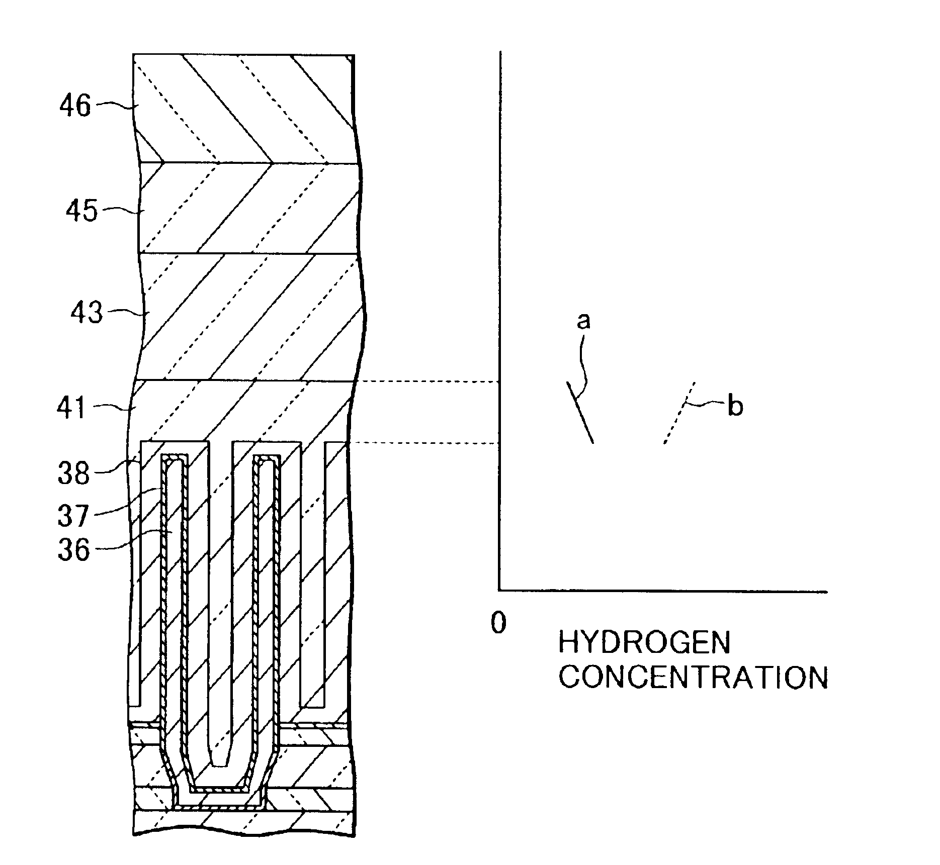
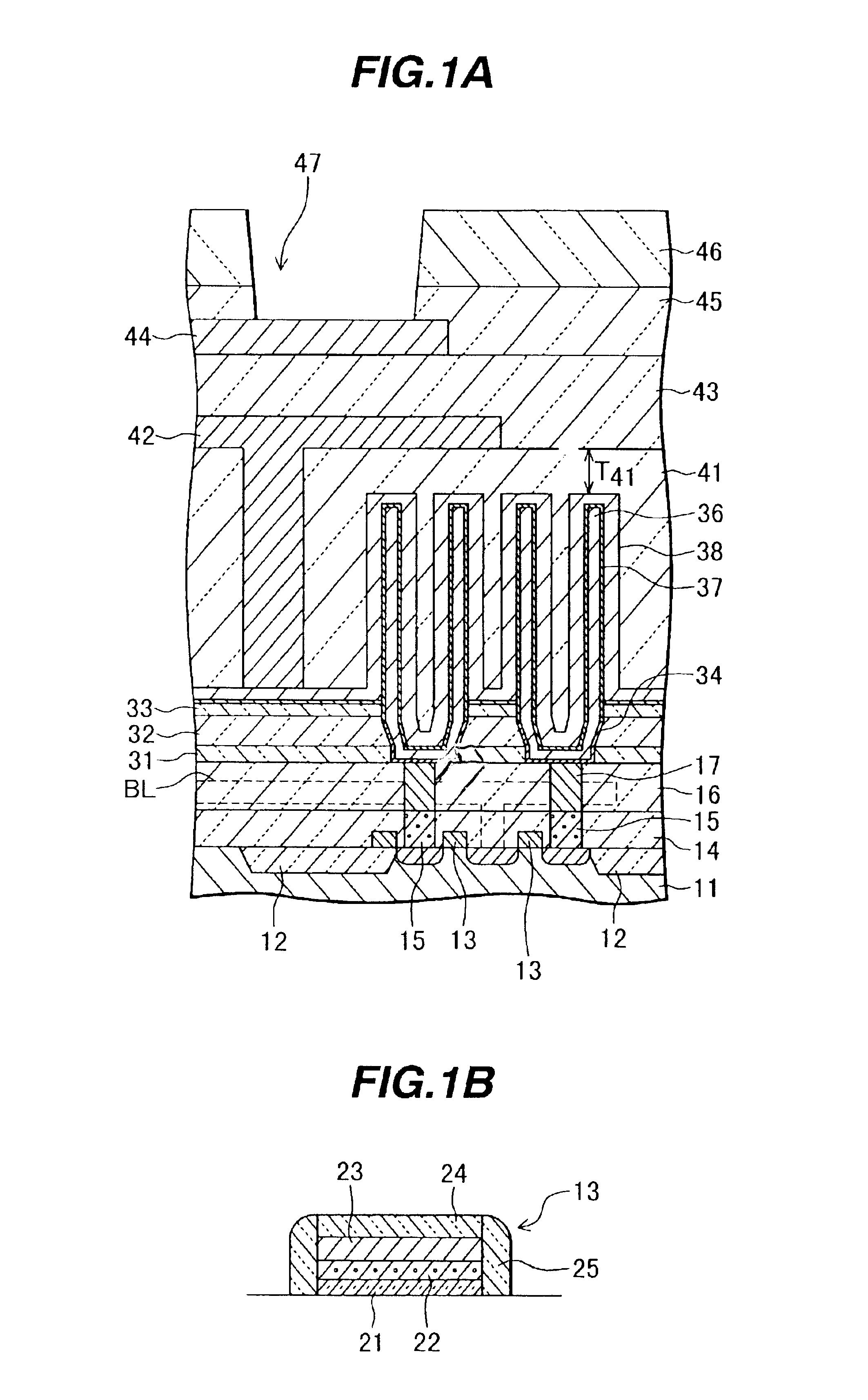
FIG. 1A is a cross sectional view of a DRAM manufactured by a semiconductor device manufacture method according to a With reference to FIG. 1A, the semiconductor device manufacture method of the embodiment will be described.

On the surface of a silicon substrate 11 having a p-type surfaces region, an isolation region 12 of silicon oxide (SiO2) is formed by shallow trench isolation (STI). An insulated gate electrode 13 is formed on the surface of an active region defined by the isolation region 12.

As shown in FIG. 1B, the insulated gate electrode 13 has: a gate insulating film 21 of silicon oxide formed on the silicon surface; a lower gate electrode 22 of polysilicon formed on the gate insulating film; an upper gate electrode 23 of tungsten silicide (WSi) or the like formed on the lower gate electrode; an etching stopper layer 24 of silicon nitride (SiN) or the like formed on the upper gate electrode; and side wall etching stoppers 25 of silicon nitride or the like covering the side ...

fifth embodiment

With reference to FIGS. 9A and 9B, a DRAM manufacture method will be described.

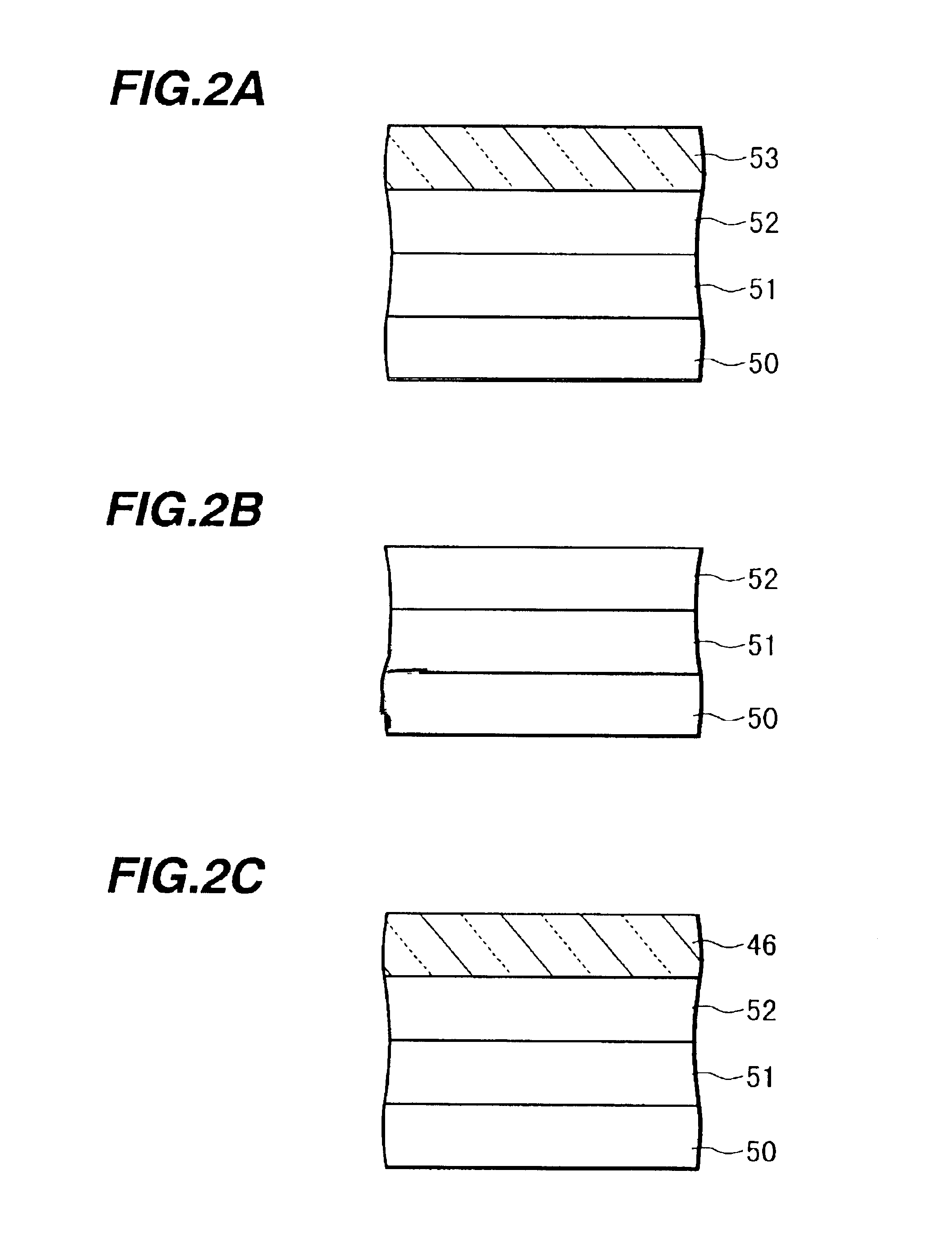
As shown in FIG. 9A, a transistor layer 50, a capacitor layer 51 and a multi-wiring layer 52 are formed. These processes are similar to those of the first embodiment described with reference to FIG. 2A. In this state, a heat treatment is performed in a hydrogen plasma atmosphere at 400 to 450° C. This heat treatment improves the transistor performance. However, since hydrogen diffuses to the capacitor layer 51, the capacitor electrical characteristic are degraded.

Before a protective film is formed, a heat treatment for improving the capacitor electrical characteristics is performed in a nitrogen atmosphere. The heat treatment conditions are the same as those of the heat treatment for improving the capacitor electrical characteristics of the first embodiment described with reference to FIG. 2B. Since the protective film is not formed, the capacitor electrical characteristics can be improved similar to the...


PUM


Abstract

On a semiconductor substrate, a transistor and a capacitor electrically connected to the transistor are formed, the capacitor having two electrodes made of metal and a capacitor dielectric layer between the two electrodes made of oxide dielectric material. A temporary protective film is formed over the capacitor, the temporary protective film covering the capacitor. The semiconductor substrate with the temporary protective film is subjected to a heat treatment in a reducing atmosphere. The temporary protective film is removed. The semiconductor substrate with the temporary protective film removed is subjected to a heat treatment in an inert gas atmosphere or in a vacuum state. A protective film is formed over the capacitor, the protective film covering the capacitor. With these processes, leak current of the capacitor can be reduced.

Description

CROSS REFERENCE TO RELATED APPLICATIONThis application is based on Japanese Patent Application No. 2002-211020, filed on Jul. 19, 2002, the entire contents of which are incorporated herein by reference.BACKGROUND OF THE INVENTION1) Field of the InventionThe present invention relates to a semiconductor device and its manufacture method, and more particularly to a semiconductor device having transistors and capacitors connected to the transistors and its manufacture method, the capacitor being made of a lamination of a metal film, a dielectric film and a metal film sequentially stacked in this order.2) Description of the Related ArtA capacitor is used as a memory element of a dynamic random access memory (DRAM). The performance of a memory element can be improved by improving the performance of a capacitor. It becomes easy to make DRAM compact if a capacitor is made of a capacitor dielectric layer having a high dielectric constant.Ta2O5 is known as oxide dielectric material having a h...

Claims


Application Information

Patent Timeline
Patent Type & Authority Patents(United States)
IPC IPC(8): H01L21/02H01L21/70H01L21/8242H01L21/314H01L21/316H01L21/322H01L27/10H01L27/108
CPCH01L27/10852H01L28/40H01L21/31604H01L28/90H01L28/55H01L27/10894H10B12/09H10B12/033H01L21/02263H01L27/10
Inventor LIN, JUNSUZUKI, TOSHIYAHIEDA, KATSUHIKO
Owner FUJITSU SEMICON LTD
Why Eureka
Try Eureka