Methods for making semiconductor structures having high-speed areas and high-density areas

Inactive Publication Date: 2005-08-11
MICRON TECH INC
View PDF11 Cites 2 Cited by
  • Summary
  • Abstract
  • Description
  • Claims
  • Application Information

AI Technical Summary

Benefits of technology

[0010] One illustrative aspect includes a method for strapping a gate structure of a transistor in a periphery area of a semiconductor structure. The method includes forming from a nonconductive stack a trench that superjacently abuts along a substantially length of a dual-doped polycrystalline silicon line having a p-type strip abutting an n-type strip. The nonconductive stack inc

Problems solved by technology

This situation allows current to undesirably flow if the diode is activated by accident in certain areas of a semiconductor structure.
This current may render a semiconductor device defective.
One of the problems with this approach is that the conductive stack 13 may promote cross-diffusion.
This movement of impurities undesirably transforms the designed semiconductor characteristic of the polycrystalline silicon.
Another problem is that certain conductive materials may decompose during processing, which forms an undesired nonconductive layer that may degrade performance of a semiconductor device.
To avoid this increase in the vertical resistance, some semiconductor manufacturers have s

Method used


Image

  • Methods for making semiconductor structures having high-speed areas and high-density areas
  • Methods for making semiconductor structures having high-speed areas and high-density areas
  • Methods for making semiconductor structures having high-speed areas and high-density areas

Examples


Embodiment Construction

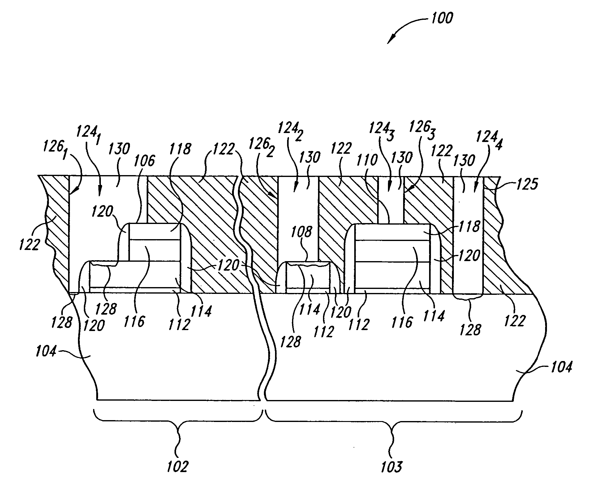
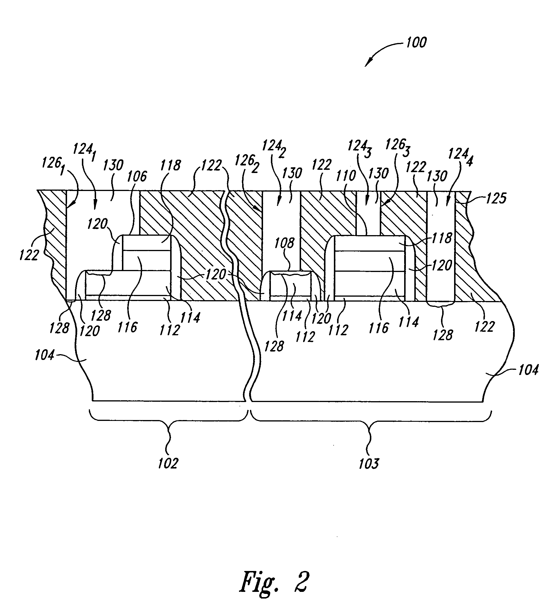
[0020] In the following detailed description of various embodiments of the invention, reference is made to the accompanying drawings, which form a part hereof, and in which are shown, by way of illustration, specific embodiments in which the invention may be practiced. In the drawings, like numerals describe substantially similar components throughout the several views. These embodiments are described in sufficient detail to enable those skilled in the art to practice the invention. Other embodiments may be utilized and structural, logical, electrical, and other changes may be made without departing from the spirit or scope of the present invention. The following detailed description is, therefore, not to be taken in a limiting sense.

[0021] A semiconductor structure, such as a memory device, may have both an array of memory cells and peripheral circuits. The array of memory cells store information, and may be referred to as an array or a storage aspect. The array may require high d...


PUM


Abstract

Methods for making a semiconductor structure are discussed. The methods include forming openings in a high-density area and a high-speed area, and forming a metallization layer simultaneously into the high-density area and the high-speed area. The metallization layer includes a combination of substances and compounds that reduce vertical resistance, reduce horizontal resistance, and inhibit cross-diffusion.

Description

TECHNICAL FIELD [0001] This invention relates generally to semiconductor structures. More particularly, it pertains to making semiconductor devices so these devices operate at high speed while having high density. BACKGROUND OF THE INVENTION [0002] In the making of certain semiconductor devices, modern semiconductor processes may require a p-type semiconductor material to be adjoined to an n-type semiconductor material, but not for the purpose of forming a diode. However, a diode is naturally formed when a p-type semiconductor material is adjoined to an n-type semiconductor material. This situation allows current to undesirably flow if the diode is activated by accident in certain areas of a semiconductor structure. This current may render a semiconductor device defective. One solution to this problem is to place a conductive material on top of the n-type semiconductor material and the p-type semiconductor material as illustrated in FIGS. 1A and 1B. [0003]FIG. 1A is a cross-sectiona...

Claims


Application Information

Patent Timeline
IPC IPC(8): H01L21/60H01L21/768H01L21/8239H01L27/105H01L27/11
CPCH01L21/76895H01L21/76897H01L27/1052H01L27/11H01L27/105H10B99/00H10B10/00
Inventor CHO, CHIH-CHENWANG, ZHONGZE
Owner MICRON TECH INC
Why Eureka
Try Eureka