Method for manufacturing transistor and semiconductor device

a manufacturing method and semiconductor technology, applied in the field of semiconductor technology, can solve the problems of affecting the significant increase of the total capacitance of the transistor, and the strong limitation of the improvement in the speed and so as to improve the performance of the transistor, reduce the damage to the formed contact layer during the process of removing at least a portion of the spacer, and reduce the capacitance

Inactive Publication Date: 2013-02-14
INST OF MICROELECTRONICS CHINESE ACAD OF SCI
View PDF4 Cites 3 Cited by
  • Summary
  • Abstract
  • Description
  • Claims
  • Application Information

AI Technical Summary

Benefits of technology

[0026]In accordance with the method for manufacturing a transistor of the present invention, after the spacer is formed to surround the gate stack or dummy gate stack, at least a portion of the spacer is removed to expose a portion of the active area, and then the gate stack or dummy gate stack, the spacer and the exposed active area are covered by the interlayer dielectric layer with a dielectric constant smaller than that of the material of the removed spacer. Namely, the original spacer material is replaced by the interlayer dielectric layer with a smaller dielectric constant, which forms the isolation between the gate region and the source / drain region as well as between the gate region and the contact plug. In fact, this reduces the dielectric constant between the gate region and the source / drain region as well as between the gate region and the contact plug, and thus makes it possible to reduce the capacitance between the gate region and the source / drain region as well as between the gate region and the contact plug, and helps to improve the performance of the transistor.
[0027]By forming the contact layer after formation of the interlayer dielectric layer, it is advantageous in that the damage to the formed contact layer during the process for removing at least a portion of the spacer is reduced.

Problems solved by technology

This may result in significant increase of the total capacitance of the transistor, which will greatly influence the speed and performance of the transistor.
As a result, the improvement in the speed and performance of the transistor is strongly limited.

Method used


Image

  • Method for manufacturing transistor and semiconductor device
  • Method for manufacturing transistor and semiconductor device
  • Method for manufacturing transistor and semiconductor device

Examples


Embodiment Construction

[0031]Firstly, it should be noted that terms regarding position and orientation mentioned in the present invention, such as “above”, “below”, etc., refer to the directions as viewed from the front of the paper in which the drawings are located. Therefore, the terms “above”, “below”, etc. regarding position and orientation in the present invention only indicate the relative positional relationship in the case as shown in the drawings. They are presented only for purpose of illustration, but not intend to restrict the scope of the present invention.

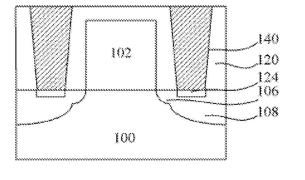
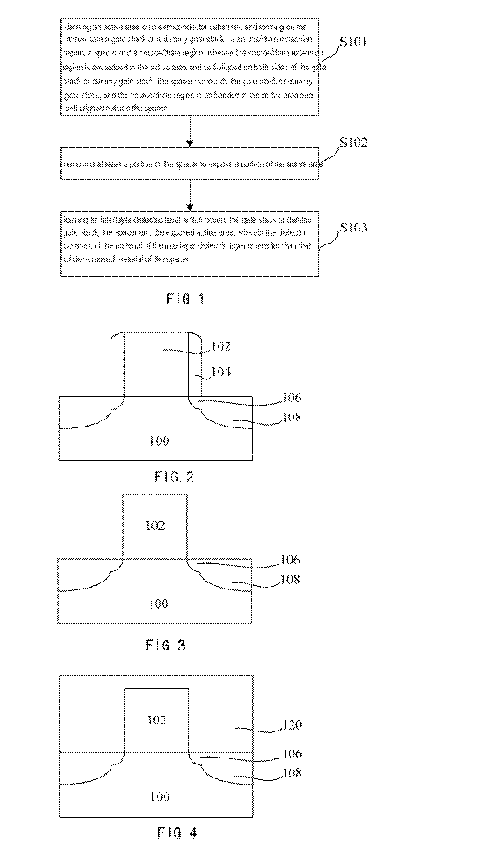
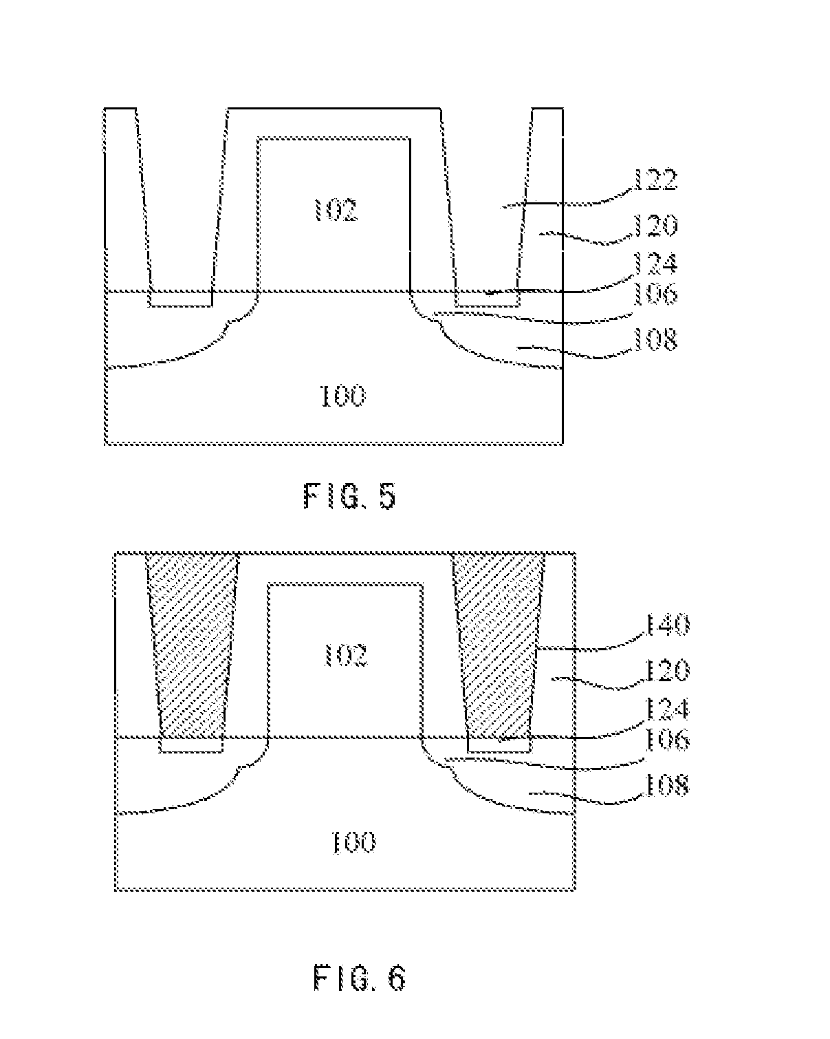
[0032]Hereinafter, the solutions provided by the present invention will be described in details with reference to the accompanying drawings. A Si substrate is shown in FIGS. 2-6 by way of example. However, in addition to Si substrate, any suitable semiconductor substrate, like SiGe substrate, III-V group elements compound substrate, silicon carbide substrate, SOI (silicon on insulator) substrate, etc., can also be used. Therefore, the prese...


PUM


Abstract

A method for manufacturing a transistor and a semiconductor device is provided. The method for manufacturing a transistor may comprise: defining an active area on a semiconductor substrate, and forming on the active area a gate stack or a dummy gate stack, a source/drain extension region, a spacer and a source/drain region, wherein the source/drain extension region is embedded in the active area and self-aligned on both sides of the gate stack or dummy gate stack, the spacer surrounds the gate stack or dummy gate stack, and the source/drain region is embedded in the active area and self-aligned outside the spacer; removing at least a portion of the spacer to expose a portion of the active area; and forming an interlayer dielectric layer which covers the gate stack or dummy gate stack, the spacer and the exposed active area, wherein the dielectric constant of the material of the interlayer dielectric layer is smaller than that of the removed material of the spacer. It is beneficial for reducing the capacitance between the gate region and the source/drain region as well as between the gate region and the contact plug.

Description

FIELD OF THE INVENTION[0001]The present invention generally relates to the semiconductor technology, and more particularly to a method for manufacturing a transistor and a semiconductor device.BACKGROUND OF THE INVENTION[0002]As transistors, like the metal oxide field effect transistor (MOSFET) are gradually decreasing in size, the distance between the gate region and the source / drain region as well as the distance between the gate region and the contact plug for the transistor is also decreasing. One can find from the formula for calculating capacitance, C=kA / d, that the capacitance is inversely proportional to the distance d, and directly proportional to the value of the dielectric constant k. This means that when the distance between the gate region and the source / drain region decreases gradually and even approaches zero, the capacitance between the gate region and the source / drain region will increase rapidly. Similarly, the capacitance between the gate region and the contact pl...

Claims


Application Information

Patent Timeline
Patent Type & Authority Applications(United States)
IPC IPC(8): H01L21/336
CPCH01L29/66545H01L29/7833H01L29/6659
Inventor YIN, HAIZHOULUO, ZHIJIONGZHU, HUILONG
Owner INST OF MICROELECTRONICS CHINESE ACAD OF SCI
Why Eureka
Try Eureka