Semiconductor device and method for forming the same

a technology of semiconductors and devices, applied in the direction of semiconductor devices, basic electric elements, electrical equipment, etc., can solve the problems of reducing the reliability of nmos transistors, and achieve the effects of increasing stresses, enhancing transistor performance, and increasing compressive stresses between epitaxial layers and channel regions

Active Publication Date: 2012-06-07
SEMICONDUCTOR MANUFACTURING INTERNATIONAL (BEIJING) CORP
View PDF6 Cites 2 Cited by
  • Summary
  • Abstract
  • Description
  • Claims
  • Application Information

AI Technical Summary

Benefits of technology

[0049]The second openings are formed by etching side walls of the first openings with the etching gas. The second openings are coupled with the first openings and located in the substrate under the first spacers, which can increases the stresses between the epitaxial layers and the channel regions, so that the performance of transistors can be enhanced. Specifically, if the transistor is a PMOS transistor, compressive stresses between the epitaxial layers and the channel regions can be increased, and if the transistor is an NMOS transistor, tensile stresses between the epitaxial layers and the channel regions can be increased.
[0050]Moreover, each of the second openings includes a side wall and an included angle between the side wall and a top surface of the substrate ranging from about 63° to about 90°. Preferably, the included angle between the side wall and the top surface of the substrate is less than 90°. And the epitaxial layers are formed by filling the first openings and the second openings. With scaling down of the dimension of semiconductor devices, the epitaxial layers formed are closer to the channel regions so that the stresses between the epitaxial layers and the channel regions can be enhanced more greatly, which can increase the migration rate of carriers, thereby promoting the response speed of semiconductor devices.
[0051]Furthermore, in the embodiments of present invention, the second openings are formed by etching the side walls of the first openings, so that the width of the spacers is not reduced, which may not affect the protective effect of the spacers on the devices which need to be protected by the spacers.

Problems solved by technology

However, the reduction of the width of the spacers located on both sidewalls of the NMOS gate structures may impair the protective effect for the NMOS gate structures, or even cause the NMOS gate structures to be exposed in the environment for forming the epitaxial layers, which may reduce the reliability of NMOS transistors.
Similarly, the problems mentioned above may exist in a process for forming epitaxial layers on both sides of the NMOS gate structure in the prior art.

Method used


Image

  • Semiconductor device and method for forming the same
  • Semiconductor device and method for forming the same
  • Semiconductor device and method for forming the same

Examples


Embodiment Construction

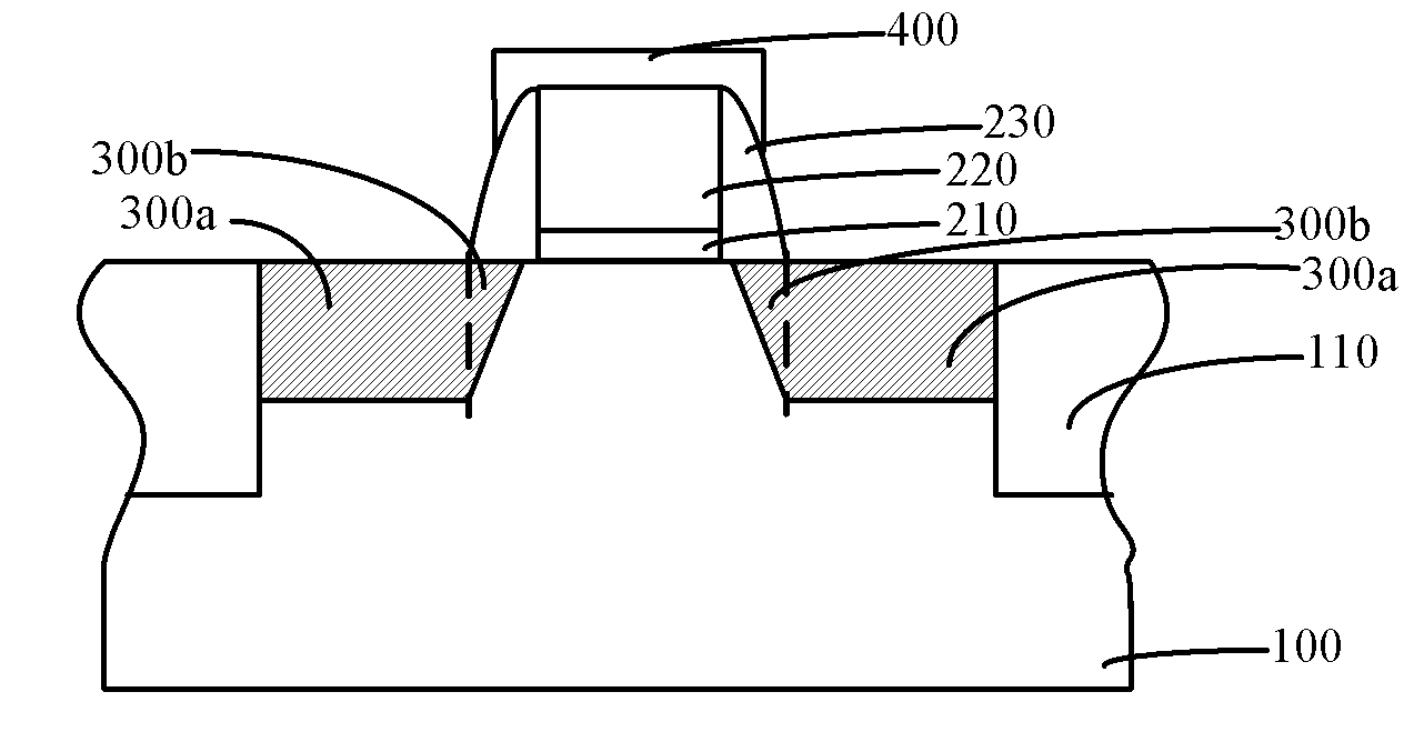
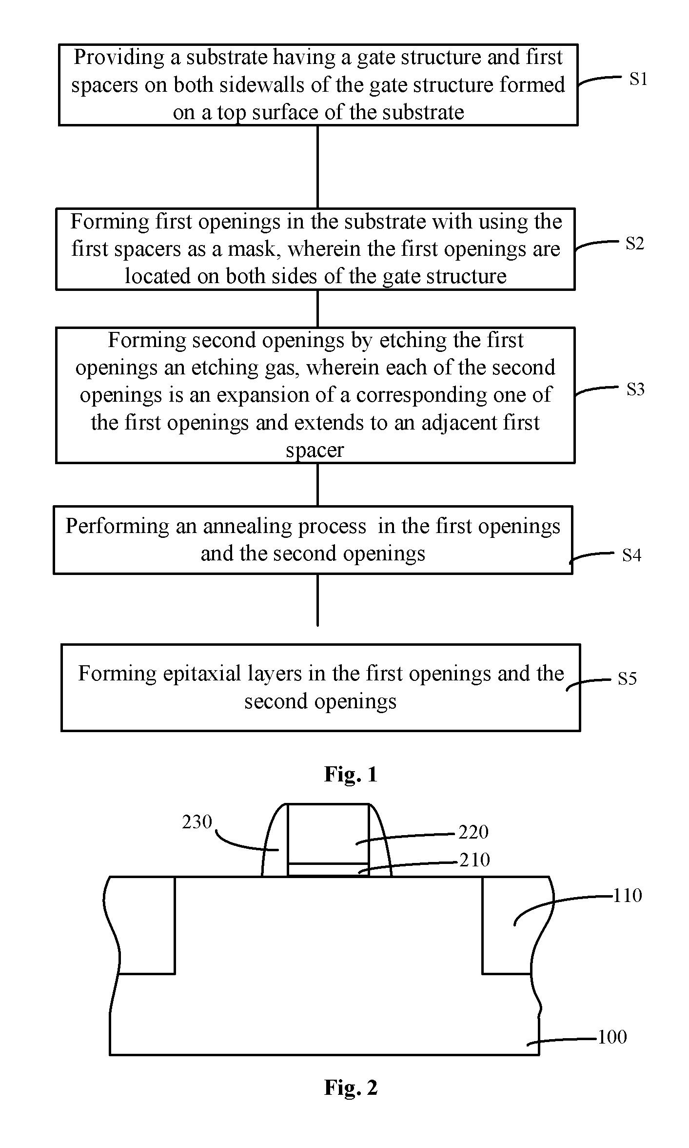
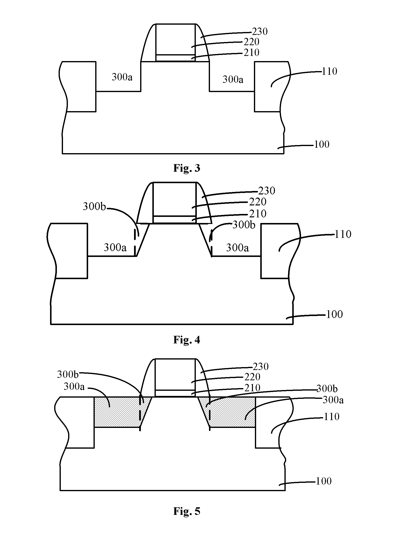
[0057]In the prior art, while forming epitaxial layers on MOS transistors, distances between two adjacent epitaxial layers can be reduced by reducing widths of spacers, so that stresses between the epitaxial layers and the channel regions of the MOS transistors are increased. However, the reduction of the widths of the spacers of some MOS transistors on which no epitaxial layers are formed may impair the protective effect for the gate structures, or even cause the gate structures to be exposed in an environment for forming the epitaxial layers, which may reduce reliability of a semiconductor device.

[0058]To solve the problems mentioned above, an embodiment of the present invention provides a method for forming a semiconductor device, including: providing a substrate, wherein a gate structure and first spacers on both sidewalls of the gate structure are formed on the substrate; forming first openings in the substrate by using the first spacers as a mask, wherein the first openings ar...


PUM


Abstract

A semiconductor device and a method for forming the same are provided. The method includes: providing a substrate having a gate structure and first spacers on both sidewalls of the gate structure formed on a top surface of the substrate; forming first openings in the substrate by using the first spacers as a mask, wherein the first openings are located on both sides of the gate structure; forming second openings by etching the first openings with an etching gas, wherein each of the second openings is an expansion of a corresponding one of the first openings toward the gate structure and extends to underneath an adjacent first spacer; and forming epitaxial layers in the first openings and the second openings.

Description

CROSS REFERENCE TO RELATED APPLICATIONS[0001]The present application claims the priority of Chinese Patent Application No. 201010569390.6, entitled “Semiconductor Device and Method for Forming the Same”, and filed on Dec. 1, 2010, the entire disclosure of which is incorporated herein by reference.FIELD OF THE INVENTION[0002]The present invention generally relates to the semiconductor manufacturing field, and more particularly, to a semiconductor device and a method for forming the semiconductor device.BACKGROUND OF THE INVENTION[0003]It is well known that carrier mobility and energy gap of silicon can be changed by a mechanical stress. And, recently, the mechanical stress plays a more and more important role in influencing performance of MOSFETs. If the carrier (electrons in NMOS transistors or holes in PMOS transistors) mobility can be increased by appropriate control of the mechanical stress, the drive current can be increased. In other words, the performance of MOSFETs can be imp...

Claims


Application Information

Patent Timeline
Patent Type & Authority Applications(United States)
IPC IPC(8): H01L21/336H01L29/78
CPCH01L21/02057H01L21/02532H01L21/0262H01L21/02639H01L29/7848H01L21/823807H01L21/823814H01L29/6653H01L29/66636H01L21/3065
Inventor HE, YOUFENG
Owner SEMICONDUCTOR MANUFACTURING INTERNATIONAL (BEIJING) CORP
Why Eureka
Try Eureka