Drive circuit, light emitting diode head, and image forming apparatus

a technology of light-emitting diodes and drive circuits, applied in the direction of pulse generators, pulse techniques, instruments, etc., can solve the problems of difficult to generate potential vref without increasing cost, difficult to eliminate a variance in property, poor printing quality, etc., to reduce the size of the ic, reduce the necessary transistor area, and reduce the power voltage

Inactive Publication Date: 2008-11-27
OKI DATA CORP
View PDF2 Cites 34 Cited by
  • Summary
  • Abstract
  • Description
  • Claims
  • Application Information

AI Technical Summary

Benefits of technology

[0118]With the configuration of the present invention, the first conductive type transistor drives the driven element. Accordingly, it is possible to drive an anode-common type driven element, thereby reducing a necessary transistor area. Further, it is possible to decrease a power voltage, and to adopt a manufacturing rule for a reduced size IC. As a result, it is possible to reduce a chip size and power consumption.

Problems solved by technology

In manufacturing the LED arrays CHP1 to CHP26, it is difficult to eliminate a variance in a property due to a lattice defect in a crystal and the likes.
When the light emitting element with a variance in a light amount is used in an LED printer as is, a variance in a printed text may occur, thereby causing poor printing quality.
In the prior art, it is difficult to generate the potential Vref without increasing cost.
Further, when a standard voltage generation circuit is used for generating a specific standard potential relative to the ground, it is difficult to drive an LED element with the anode-common arrangement with a simple circuit.
With the configuration disclosed in Patent Reference 2, it is necessary to provide a plurality of calculation amplifiers, thereby increasing a chip area and cost.
However, in the prior art, it is difficult to solve the issue associated with the second difference.
Accordingly, it is difficult to maintain the current-mirror relationship between the PMOS transistor 56 and the PMOS transistor Tr1, thereby making it difficult to normally operate the circuit shown in FIG. 21.
However, when the power voltage is 3.3 V, it is difficult to operate the circuit.
However, in the prior art, it is difficult to obtain a circuit without increasing cost.
For this reason, while the LED head shown in FIG. 21 has been commercialized, it is difficult to realize the configuration shown in FIG. 22.

Method used


Image

  • Drive circuit, light emitting diode head, and image forming apparatus
  • Drive circuit, light emitting diode head, and image forming apparatus
  • Drive circuit, light emitting diode head, and image forming apparatus

Examples


first embodiment

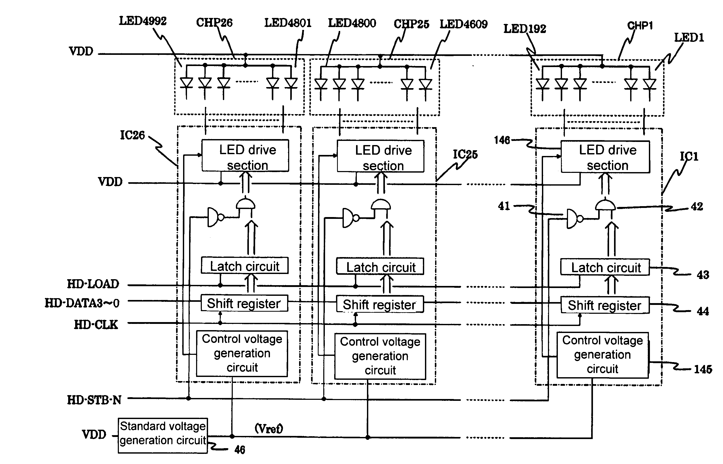
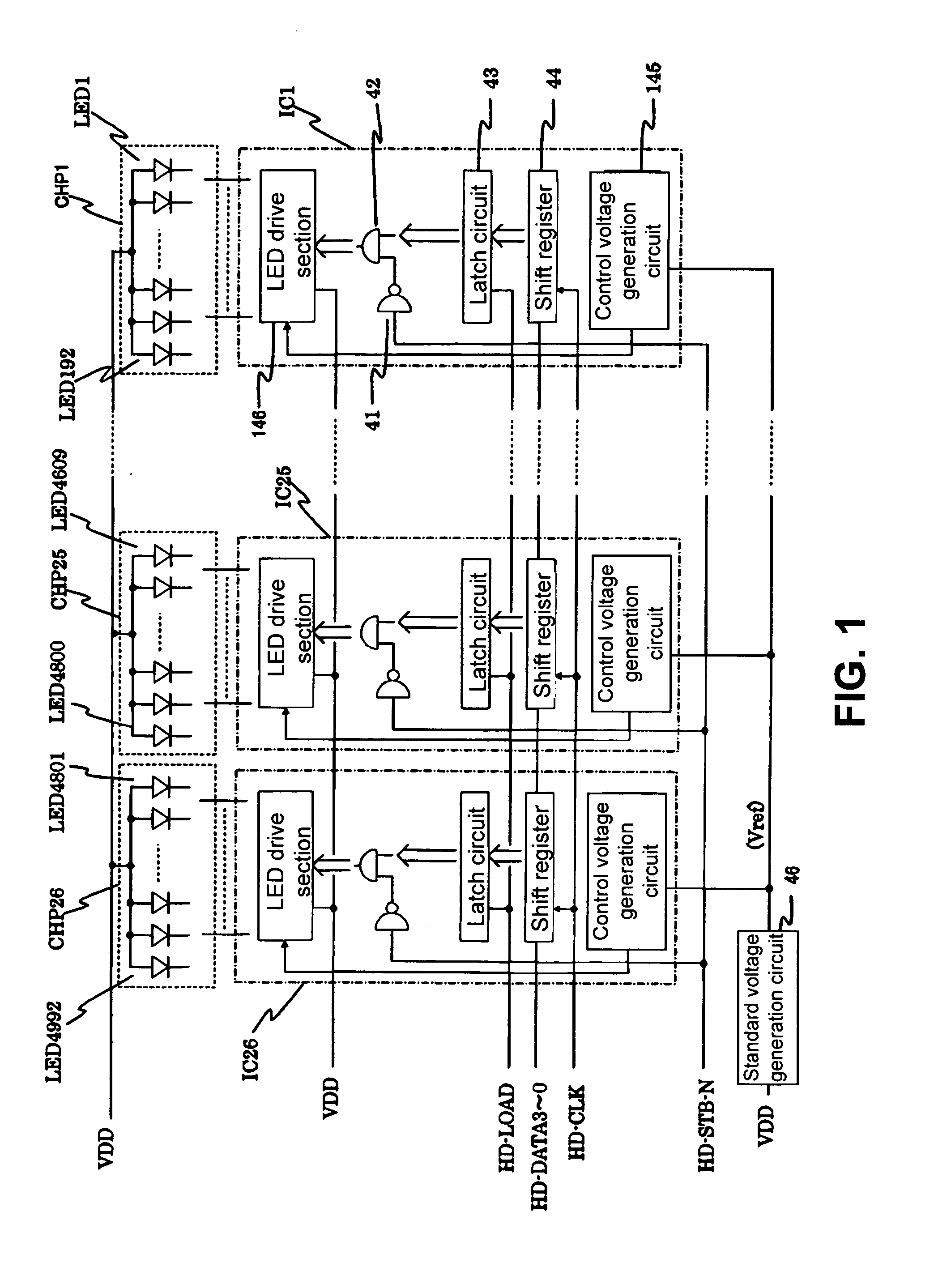
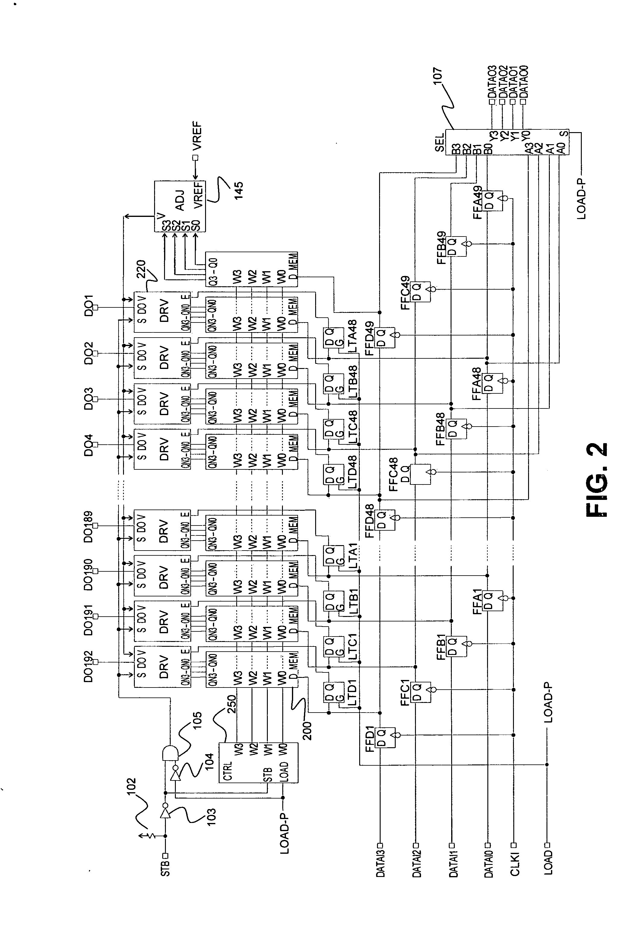
[0146]A first embodiment of the present invention will be explained. FIG. 1 is a block diagram showing a configuration of an LED (Light Emitting Diode) head of an electro-photography printer according to the first embodiment of the present invention. FIG. 2 is a block diagram showing a configuration of a driver IC (Integrated Circuit) of the LED head according to the first embodiment of the present invention.

[0147]As shown in FIG. 1, the LED head includes 26 LED arrays CHP1 to CHP26, and each of the LED arrays CHP1 to CHP26 includes 192 LED elements (for example, LED elements LED1 to LED192 are disposed in the LED array CHP1). In the LED array, an anode terminal of each of the LED elements is connected to with each other, thereby constituting an anode-common arrangement.

[0148]In the embodiment, driver ICs IC1 to IC26 in the same number as that of the LED arrays are arranged to correspond to the LED arrays. Each of the driver IC IC1 to IC26 includes a control voltage generation circu...

second embodiment

[0246]A second embodiment of the present invention will be explained next. FIG. 11 is a block diagram showing a configuration of a driver IC according to the second embodiment of the present invention. The driver IC is provided for driving an LED array (not shown). Accordingly, the driver IC supplies a drive current to an anode terminal of an LED element (not shown), so that the drive current flows to ground through a cathode terminal of the LED element, thereby emitting light.

[0247]Similar to the first embodiment, the shift register 44 is formed of flip-flop circuits FFA1 to FFA49, FFB1 to FFB49, FFC1 to FFC49, and FFD1 to FFD49 shown in FIG. 11. Further, corresponding to the latch circuit 43 in the first embodiment, the latch circuits LTA1 to LTD1, to LTS49 to LTD49 are provided. The control circuit 250 (CTRL) has a configuration similar to that in the first embodiment.

[0248]As shown in FIG. 11, the IC driver includes memory circuits 300 (described later) and LED drive circuits 37...

third embodiment

[0337]A third embodiment of the present invention will be explained next. FIG. 24 is a schematic view showing an LED head 500 according to the third embodiment of the present invention. As shown in FIG. 24, an LED unit 502 is mounted on a base member 501. In the LED unit 502, the circuits shown in FIG. 17 and the likes are mounted on a mounting board.

[0338]FIG. 25 is a schematic plan view showing the LED unit 502 according to the third embodiment of the present invention. As shown in FIG. 25, in the LED unit 502, a plurality of circuits 502a formed of the light emitting portions (CHP1 to CHP26) and the drive circuits (IC1 to IC26) described above is arranged on a mounting substrate 502e along a longitudinal direction thereof. On the mounting substrate 502e, there are disposed electrical device mounting areas 502b and 502c for mounting electrical devices and wiring patterns, and a connector 502d for supplying a control signal and power from outside.

[0339]As shown in FIG. 23, a rod le...


PUM


Abstract

A drive circuit includes a drive element for driving a driven element; a correction data input section for adjusting a drive current of the driven element; a resistor having an end portion connected to ground; and a control voltage generation section for generating a direction value of the drive current. The control voltage generation section includes a calculation amplifier having a first input terminal for receiving a standard voltage, a second input terminal, and an output terminal; a first conductive type transistor having a first terminal, a second terminal connected to the ground, and a control terminal connected to the output terminal; and a current-mirror circuit including a control side transistor and a follower side transistor. The control side transistor has a current output terminal connected to the first terminal. The follower side transistor has a current output terminal connected to another end portion of the resistor and the second input terminal.

Description

BACKGROUND OF THE INVENTION AND RELATED ART STATEMENT[0001]The present invention relates to a drive circuit for driving a group of driven elements such as, for example, an array of light emitting diodes (LEDs) disposed in an electro-photography printer as a light source, an array of heating resistors disposed in a thermal printer, and an array of display units disposed in a display device. The present invention also relates to a light emitting diode (LED) head including the drive circuit; and an image forming apparatus including the light emitting diode (LED) head.[0002]In the specification, a light emitting diode may be referred to as an LED; a monolithic integrated circuit may be referred to as an IC; an n-channel MOS (Metal Oxide Semiconductor) transistor may be referred to as an NMOS (transistor); and a p-channel MOS transistor may be referred to as a PMOS (transistor).[0003]Further, a high signal level may be referred to as a logical value of one (1), and a low signal level may...

Claims


Application Information

Patent Timeline
Patent Type & Authority Applications(United States)
IPC IPC(8): G03G15/043H05B37/02G05F1/10
CPCG03G2215/0409G09G3/32G09G2320/0233G03G15/04054H05B33/0827H05B33/0845G09G2330/028B41J2/45H05B45/46H05B45/18
Inventor NAGUMO, AKIRA
Owner OKI DATA CORP
Why Eureka
Try Eureka